Introduction
Printed Circuit Board (PCB) design is a critical aspect of modern electronics, where the arrangement of signal layers directly impacts performance, reliability, and manufacturability. For electrical engineers, mastering signal layer best practices and PCB layering techniques is essential to ensure signal integrity, minimize electromagnetic interference (EMI), and streamline design for manufacturing. A well planned layer stackup not only optimizes routing strategies but also enhances signal layer optimization for high speed and mixed signal applications. This article dives into the technical principles of PCB layering, offers actionable strategies for EMI reduction, and provides insights into creating robust designs. Whether you are working on consumer electronics or industrial systems, understanding these concepts will elevate your PCB projects to meet stringent performance standards.
What Are Signal Layers and Why Do They Matter
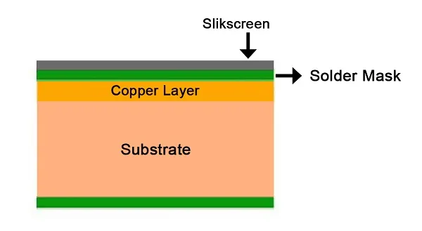
Signal layers in a PCB are conductive planes dedicated to carrying electrical signals between components. These layers are typically made of copper and are sandwiched between insulating materials within the board stackup. Their primary role is to facilitate communication between circuit elements while maintaining signal integrity. Poorly designed signal layers can lead to crosstalk, signal degradation, and increased EMI, which compromise device functionality.
The importance of signal layers becomes evident in high speed designs where timing and impedance control are critical. Proper PCB layering techniques ensure minimal noise coupling and provide stable reference planes for signals. For electrical engineers, optimizing signal layers is not just about functionality but also about meeting industry standards for performance and reliability. A strategic approach to layer arrangement directly influences the success of the final product in terms of both operation and compliance.
Technical Principles of Signal Layer Design
Layer Stackup Fundamentals
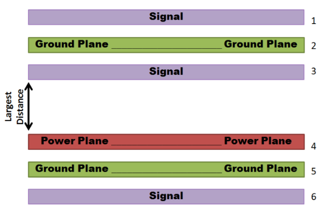
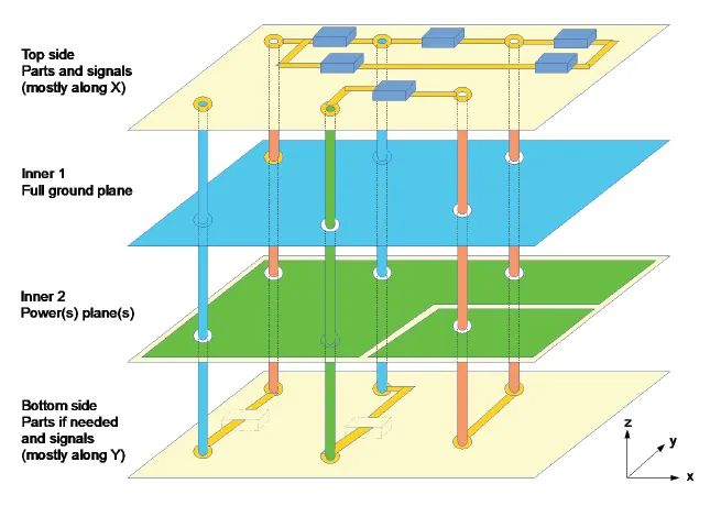
A PCB stackup refers to the arrangement of conductive and insulating layers within the board. Signal layers are often paired with ground or power planes to provide a return path for currents and to shield against interference. The stackup design must account for the type of signals, such as digital, analog, or mixed, as well as the operating frequency. In high speed applications, controlled impedance is achieved by maintaining consistent spacing between signal layers and their reference planes.
Signal Integrity and Impedance Control
Signal integrity is the cornerstone of effective PCB design. It ensures that signals maintain their intended shape and timing as they travel through the board. Impedance mismatches can cause reflections, leading to data errors or signal loss. Engineers must calculate trace widths and layer spacing to match the characteristic impedance, often guided by standards like IPC-2141A for controlled impedance design. Proper stackup symmetry also prevents board warpage during manufacturing.
EMI and Crosstalk Considerations
Electromagnetic interference occurs when unwanted signals couple into sensitive circuits, often due to poor layer separation or inadequate grounding. Crosstalk happens when adjacent traces or layers interfere with each other. Both issues can be mitigated by placing ground planes between signal layers, ensuring tight coupling to reference planes, and maintaining adequate spacing between high speed traces. These principles form the basis for EMI reduction in PCB design.
Related Reading: High Frequency PCB Routing Techniques: Minimizing Signal Loss and Interference
Practical Solutions for Signal Layer Optimization
Best Practices for Layer Arrangement
Effective PCB layering techniques start with a logical stackup. For a four layer board, a common configuration includes signal layers on the top and bottom, with internal ground and power planes. This setup provides shielding and stable reference for signals. In six or eight layer designs, additional signal layers can be added, but they should alternate with ground planes to minimize noise coupling. Always prioritize symmetry to avoid mechanical stress during fabrication.
- Place high speed signals on layers adjacent to ground planes for better return paths.
- Keep analog and digital signals on separate layers to prevent interference.
- Use continuous ground planes without splits to maintain low impedance return paths.
Routing Strategies for Signal Integrity
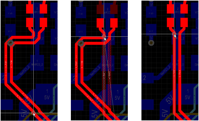
Routing strategies play a vital role in signal layer best practices. High speed traces should be kept short and direct to minimize delay and reflections. Avoid routing over splits in ground planes, as this disrupts the return path and increases EMI. Differential pairs, common in high speed designs, must maintain equal length and consistent spacing to ensure timing alignment. Adhering to guidelines in standards like IPC-2221B for generic PCB design can help achieve reliable routing.
- Route critical signals first to secure optimal paths.
- Minimize vias for high speed signals to reduce inductance.
- Use 45 degree angles instead of sharp corners to prevent signal reflection.
Techniques for EMI Reduction
EMI reduction is a priority in modern PCB design, especially for applications in sensitive environments. Beyond layer arrangement, engineers can employ additional strategies to suppress interference. Adding ground stitching vias around the board edges creates a Faraday cage effect, containing radiated emissions. Decoupling capacitors placed close to power pins of integrated circuits help filter noise. These techniques, when combined with proper stackup, significantly lower EMI risks.
- Space traces adequately to avoid crosstalk between adjacent signals.
- Use ground pours on signal layers to shield traces and reduce noise.
- Implement common mode chokes for power lines to filter conducted emissions.
Related Reading: Signal Integrity PCB Designers
Design for Manufacturing Considerations
Signal layer optimization must align with design for manufacturing principles to ensure producibility. Overly complex stackups or tight tolerances can increase fabrication costs and lead to defects. Engineers should consult standards like IPC-6012E for rigid board performance specifications to define achievable layer counts and material properties. Communication with fabricators during the design phase helps identify constraints and adjust the stackup for better yield.
- Limit layer count to balance cost and performance needs.
- Specify standard dielectric materials to avoid supply chain delays.
- Ensure trace widths and clearances meet fabrication capabilities per IPC-A-600K.
Troubleshooting Common Signal Layer Issues
Electrical engineers often encounter challenges with signal layers during design validation or testing phases. One frequent issue is unexpected noise in high speed circuits, often traced back to inadequate grounding or split planes. Inspecting the stackup for continuous reference planes and adding ground vias can resolve this. Another problem is signal delay mismatches in differential pairs, which can be corrected by rerouting traces to equalize lengths.
In mixed signal designs, analog and digital interference is a common concern. Separating these signals onto different layers, with a solid ground plane in between, prevents coupling. If board space is limited, careful partitioning of zones on the same layer, combined with ground shielding, can mitigate risks. Referencing standards like IPC-2223D for sectional design aids in addressing such layout challenges systematically.
Conclusion
Mastering signal layer strategies is fundamental to achieving PCB success in today’s complex electronic designs. By adhering to signal layer best practices and employing effective PCB layering techniques, electrical engineers can optimize performance and ensure reliability. Strategic routing, thoughtful stackup design, and targeted EMI reduction measures collectively enhance signal integrity while aligning with design for manufacturing goals. As technology advances, staying informed about evolving standards and practices remains crucial. A disciplined approach to signal layer optimization not only meets project requirements but also sets the foundation for innovation in electronics development.
FAQs
Q1: What are the key signal layer best practices for high speed PCB design?
A1: For high speed PCB design, prioritize placing signal layers adjacent to continuous ground planes for stable return paths. Keep trace lengths short, avoid routing over plane splits, and maintain controlled impedance per industry standards like IPC-2141A. Use differential pair routing with matched lengths to prevent timing issues. These steps ensure signal integrity and minimize noise.
Q2: How do PCB layering techniques impact EMI reduction?
A2: PCB layering techniques significantly influence EMI reduction by providing shielding through ground planes between signal layers. A well planned stackup isolates high speed signals, reducing crosstalk and radiated emissions. Ground stitching vias and proper trace spacing further suppress interference. Following guidelines in standards like IPC-2221B helps achieve effective EMI control in layouts.
Q3: What routing strategies should engineers use for signal layer optimization?
A3: Engineers should route critical signals first to secure optimal paths, minimize vias to reduce inductance, and avoid sharp corners by using 45 degree bends. Differential pairs must maintain equal lengths and spacing. Keeping traces short and direct, while referencing ground planes, enhances signal layer optimization and supports robust performance in high speed designs.
Q4: How does design for manufacturing relate to PCB signal layer planning?
A4: Design for manufacturing ensures signal layer planning aligns with fabrication capabilities, avoiding overly complex stackups that increase costs or defects. Specifying standard materials and adhering to tolerances in standards like IPC-6012E improves yield. Early collaboration with fabricators helps adjust layer counts and clearances for practical production without compromising design goals.
References
IPC-2141A — Design Guide for High Speed Controlled Impedance Circuit Boards. IPC, 2004.
IPC-2221B — Generic Standard on Printed Board Design. IPC, 2012.
IPC-2223D — Sectional Design Standard for Flexible/Rigid-Flexible Printed Boards. IPC, 2016.
IPC-6012E — Qualification and Performance Specification for Rigid Printed Boards. IPC, 2020.
IPC-A-600K — Acceptability of Printed Boards. IPC, 2020.