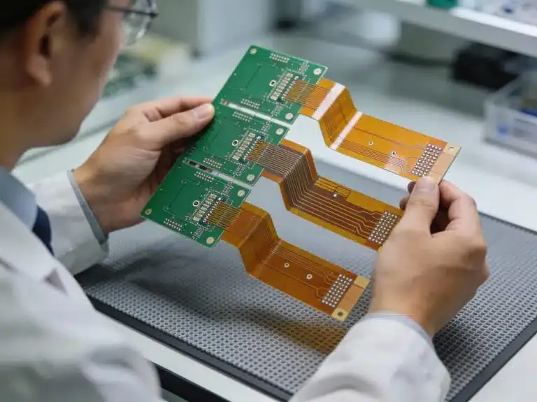
Introduction
Aluminum PCBs offer electronic hobbyists a reliable way to manage heat in projects like LED lighting arrays, audio amplifiers, and power supplies. Unlike standard FR4 boards, these metal core printed circuit boards use an aluminum substrate to efficiently dissipate thermal energy from components. Hobbyists often encounter overheating issues in high-power designs, and aluminum PCBs address this by providing superior thermal conductivity. This guide walks you through the essentials of aluminum PCB design, from understanding the structure to creating layouts suitable for prototyping. By following structured steps, beginners can produce functional boards that perform well under load. Whether you are building a custom LED driver or a motor controller, mastering aluminum PCB basics will elevate your projects.
What Is an Aluminum PCB and Why Does It Matter for Hobbyists?
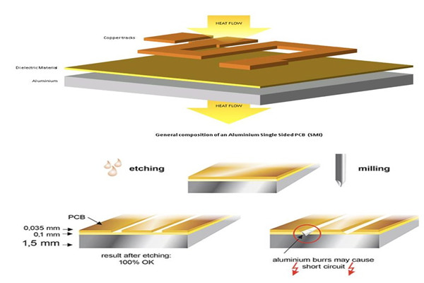
An aluminum PCB consists of a base layer of aluminum, a thin electrically insulating dielectric layer, and a top copper circuit layer. The aluminum core acts as a built-in heat sink, spreading heat away from power components much faster than traditional materials. For hobbyists working on projects with LEDs or transistors that generate significant heat, this design prevents failures and extends component life. Standard FR4 PCBs rely on air cooling or added heatsinks, but aluminum versions integrate thermal management directly into the board. This makes them ideal for compact builds where space is limited. In hobbyist applications, such as automotive lighting prototypes or guitar pedal amps, aluminum PCBs ensure reliability without complex cooling setups.
The relevance grows as hobby projects scale in power. For instance, a simple LED strip driver on FR4 might warp or delaminate under prolonged use, while an aluminum PCB maintains integrity. Hobbyists benefit from lower costs compared to advanced cooling solutions and easier assembly. These boards support through-hole and surface-mount components, fitting common prototyping workflows. Overall, adopting aluminum PCBs empowers beginners to tackle thermal challenges confidently.
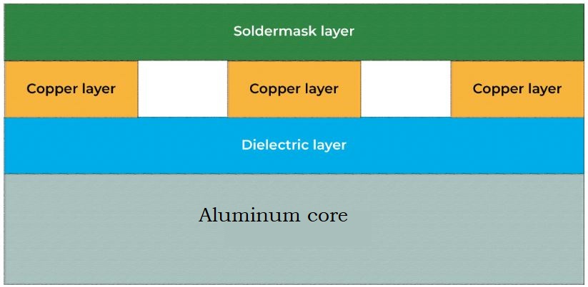
Aluminum PCB Stackup: Single Layer vs. Double Layer
The aluminum PCB stackup defines how layers interact for electrical and thermal performance. A single layer aluminum PCB features one copper layer on the dielectric atop the aluminum base, with components mounted only on the top side. This configuration suits simple hobby projects needing basic routing and maximum heat transfer. Typical thicknesses include 1 to 2 mm aluminum core, 100 to 150 micron dielectric, and 1 oz copper foil. Heat from components flows directly through the thin dielectric to the aluminum, which can then attach to an external heatsink.
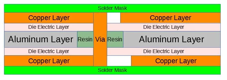
Double layer aluminum PCBs add a second copper layer beneath the first, separated by additional dielectric, still on the aluminum base. Components remain on one side, but the extra layer allows signal routing on the inner plane. This setup handles more complex circuits, like those with control signals alongside power paths. However, thermal transfer slightly decreases due to the added layers, so designers prioritize short paths from heat sources to the core.
- Single Layer Aluminum PCB — Layers: Aluminum base + Dielectric + 1 Copper; Typical hobby uses: LED arrays, power resistors; Thermal path efficiency: Highest, direct to core.
- Double Layer Aluminum PCB — Layers: Aluminum base + Dielectric + 2 Copper (with inner dielectric); Typical hobby uses: Amplifiers with feedback loops; Thermal path efficiency: Good, with vias for heat.
Understanding stackup choices prevents common pitfalls. Single layer suits pure power dissipation, while double layer offers routing flexibility. Always specify stackup details when ordering prototypes to match your design intent.
Selecting Aluminum PCB Design Software for Beginners
Electronic hobbyists need accessible aluminum PCB design software that handles metal core specifics without steep learning curves. Free open-source tools provide schematic capture, layout editing, and Gerber output tailored for prototyping services. Look for software supporting custom stackups, thermal via arrays, and copper pour features essential for aluminum boards. These platforms often include libraries for common power components like LEDs and MOSFETs. Beginners should prioritize intuitive routing tools and 3D previews to visualize heat spread.
Start with software that allows defining board outlines matching aluminum sheet sizes, typically rectangular for cost efficiency. Import footprints for through-hole mounting holes, crucial for heatsink attachment. Simulation plugins for basic thermal analysis help validate designs early. Community forums offer templates for aluminum PCB projects, speeding up your workflow. With practice, you can iterate layouts quickly, testing variations in trace widths for current handling.
Step-by-Step Aluminum PCB Layout Tutorial
Begin your aluminum PCB layout tutorial by creating a new project in your chosen design software. Draw the schematic first, placing power components centrally over areas planned for thick copper pours. Generate the netlist and transfer to the PCB editor, setting the board outline to fit standard panel sizes. Define the aluminum PCB stackup by selecting metal core preset or custom layers, ensuring the dielectric thickness aligns with thermal needs.
Route high-current traces wide, at least 2 mm for 5A paths, connecting directly to component pads. Add thermal vias under heat-generating parts, arrayed in 0.3 mm diameter holes filled with solder or epoxy for conductivity. Use copper pours on unused areas, tied to the aluminum base via vias, to spread heat evenly. Place mounting holes at corners and under major components, oversized for M3 screws to secure heatsinks.
Review for IPC-2221 design guidelines, checking clearances and annular rings. Run design rule checks for minimum trace width and via spacing. Export Gerbers, drill files, and stackup drawings for fabrication. Prototype a single layer aluminum PCB first to test, then advance to double layer for complexity.
Finalize with silkscreen labels for polarity and test points. This process ensures your layout supports reliable thermal performance.
Best Practices for Aluminum PCB Design and Thermal Management
Prioritize component placement with high-power devices over the aluminum core center for uniform heat distribution. Wide traces and polygons minimize resistance and voltage drop in power paths. Thermal vias enhance conduction from copper to base, spaced tightly under dies but avoiding solder mask plug issues.
Adhere to IPC-6012 performance specifications for plating and hole quality, ensuring vias conduct heat effectively. Avoid routing signals across expansion seams, as aluminum coefficients differ from copper. For double layer aluminum PCB, ground the inner plane to shield and aid cooling.
Mechanical design includes chamfered edges to prevent warpage during soldering. Test prototypes with IR thermography to verify hotspots. These practices align with J-STD-020 handling for assembly reliability.
Troubleshooting Common Aluminum PCB Issues
Hobbyists often face warpage from uneven heating, mitigated by symmetric layouts and controlled soldering profiles. Poor thermal transfer signals thin dielectric or unfilled vias, addressed by specifying high-conductivity insulators. Signal integrity in double layers improves with stitching vias.
Delamination risks rise in humid environments, so bake boards per IPC-A-600 acceptability criteria before assembly.
Conclusion
Designing an aluminum PCB empowers hobbyists to build robust, heat-resistant projects efficiently. From grasping stackups to applying layout best practices, this guide provides a logical path forward. Start with single layer aluminum PCB for simplicity, experiment with software tools, and iterate based on thermal tests. Standards like IPC guidelines ensure professional results. Embrace these techniques to enhance your electronics creations.
FAQs
Q1: What is the best aluminum PCB design software for electronic hobbyists?
A1: Free open-source aluminum PCB design software offers schematic and layout tools ideal for beginners. These programs support custom stackups and thermal features without cost barriers. Hobbyists appreciate 3D views for heatsink fitment. Download one with active communities for tutorials and libraries. This setup streamlines prototyping high-power boards effectively.
Q2: Can you provide an aluminum PCB layout tutorial for single layer designs?
A2: Follow a step-by-step aluminum PCB layout tutorial: schematic to PCB transfer, wide power traces, thermal vias, copper pours. Place components over core center. Define single layer aluminum PCB stackup with thin dielectric. Run DRCs per design rules. Export files ready for fab. Test for heat spread.
Q3: How does a double layer aluminum PCB differ from single layer?
A3: A double layer aluminum PCB adds an inner copper plane for routing flexibility while maintaining aluminum core cooling. Components mount on one side, unlike fully double-sided. Use for mixed power-signal hobby projects. Thermal vias bridge layers to base. Stackup complexity increases slightly. Ideal when single layer limits traces.
Q4: What should I know about aluminum PCB stackup for thermal performance?
A4: Aluminum PCB stackup prioritizes thin, high-conductivity dielectric between copper and base. Single layer offers direct heat path, double layer needs vias. Specify thicknesses for prototypes. Align with thermal needs of LEDs or amps. Uniform pours aid dissipation. Review for fab compatibility early.
References
IPC-2221B — Generic Standard on Printed Board Design. IPC, 2012
IPC-6012E — Qualification and Performance Specification for Rigid Printed Boards. IPC, 2017
IPC-A-600K — Acceptability of Printed Boards. IPC, 2020