Introduction
High-layer-count printed circuit boards form the backbone of modern electronics, enabling dense interconnects in applications like servers, aerospace systems, and telecommunications equipment. These boards typically feature 20 or more layers to support complex signal routing and power distribution. Vias serve as critical pathways for electrical connections between layers, but in dense multilayer stacks, unfilled vias can lead to mechanical weaknesses and reliability concerns during fabrication and operation. PCB filled vias mitigate these issues by completely filling the via hole with specialized materials, enhancing overall board performance. This approach aligns with the demands of high-reliability PCB designs where failure is not an option. Engineers designing such boards must understand how filled vias contribute to structural integrity and long-term functionality.
What Are PCB Filled Vias and Why Do They Matter in High-Layer-Count PCBs
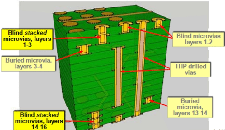
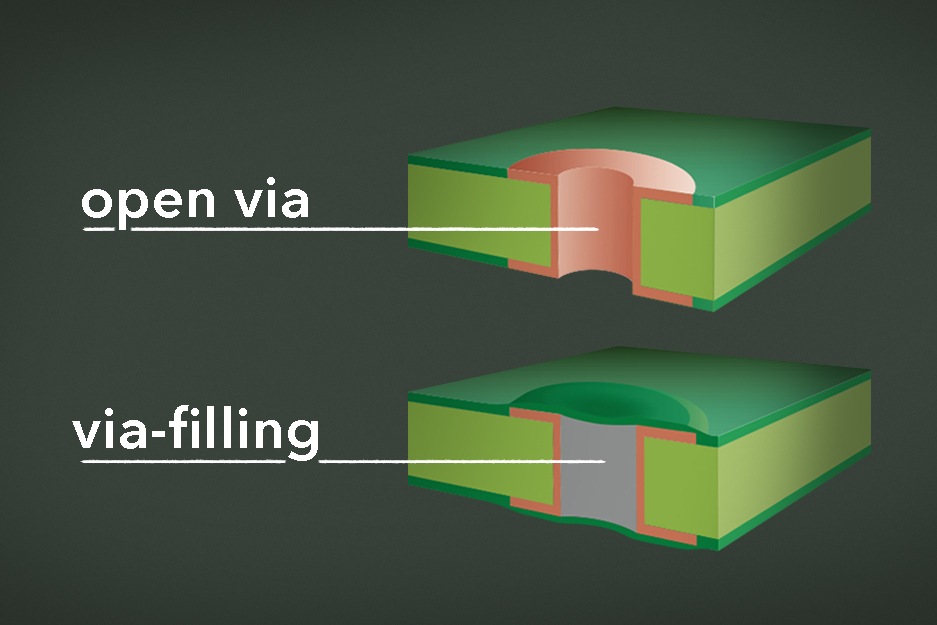
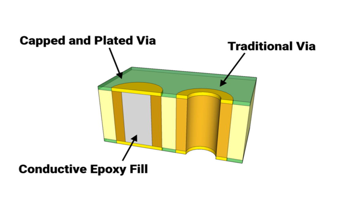
PCB filled vias consist of plated through-holes or microvias that are entirely filled with conductive or non-conductive materials after plating, eliminating the internal air gap. Conductive fills, such as copper or silver epoxy, maintain electrical continuity while non-conductive options like epoxy resin provide mechanical support without adding parallel paths. In high-layer-count PCBs, the accumulation of numerous vias increases susceptibility to warpage due to coefficient of thermal expansion mismatches between copper plating and the surrounding laminate. Unfilled vias act as stress concentrators, exacerbating cracks during thermal cycling or mechanical shock. Filled vias restore uniform CTE across the via structure, closely matching the base material and reducing these risks. Their importance grows in boards with tight BGA pitches or stacked microvias, where reliability directly impacts system uptime.
The relevance stems from evolving design requirements for miniaturization and higher speeds. Factory processes for high-layer-count boards involve multiple lamination cycles, which amplify via reliability challenges. Standards like IPC-4761 outline via protection strategies, classifying filled vias as a robust option for demanding environments. Without filling, vias may trap plating chemicals or moisture, leading to corrosion or delamination over time. For electrical engineers, specifying filled vias ensures compliance with performance criteria in multilayer constructions. Ultimately, they enable higher routing density without compromising board flatness or interconnect stability.
Technical Principles Behind the Benefits of Filled Vias
Filled vias enhance mechanical strength by distributing stresses evenly across the filled cross-section, preventing barrel cracking common in unfilled structures. During lamination and reflow, the filler material bonds tightly to the copper plating, creating a solid composite that resists shear forces from layer expansion. This is particularly vital in high-layer-count PCBs, where core-to-core alignment relies on via stability through sequential builds. Non-conductive fills approximate the laminate's CTE, minimizing warpage that could misalign outer layers. Conductive fills add redundancy for power vias, improving current carrying capacity under high loads.
Thermal management improves significantly as filled vias eliminate air voids, which act as insulators with low thermal conductivity. The filler materials, often epoxy-based, offer thermal conductivities closer to FR-4 laminates, facilitating better heat spreading from inner power planes. In multilayer stacks, this reduces hotspot formation during operation, extending component life. Electrical performance benefits include lower inductance for signal vias, as the solid fill reduces parasitic effects in high-speed designs. EMI reduction occurs because filled vias present a uniform impedance profile, minimizing reflections at layer transitions. IPC-6012 performance specifications highlight how such enhancements support qualification testing for rigid boards under thermal stress.
From a fabrication perspective, via filling prevents issues like chemical entrapment during solder masking or assembly fluxes. High-aspect-ratio vias in dense boards are prone to incomplete drainage, but filling seals them completely. This process also strengthens pad-to-via interfaces, reducing lift-off risks in fine-pitch arrays. For high-reliability PCBs, these principles translate to fewer field failures, as verified through accelerated life testing protocols.
Key Benefits of Using Filled Vias in High-Layer-Count Designs
One primary benefit is superior mechanical reliability, where filled vias withstand repeated thermal excursions without fracturing. In high-layer-count PCBs, boards undergo multiple press cycles, and unfilled vias contribute to cumulative warpage exceeding acceptable limits. Filling mitigates this by providing a monolithic structure that maintains planarity, crucial for subsequent SMT processes. Engineers report fewer rejects in production due to via-related defects when filling is employed strategically.
Thermal dissipation stands out as another advantage, especially for power distribution vias. Conductive via filling materials like copper electroplating extend heat paths vertically through the stackup, equalizing temperatures across layers. This is essential in applications with high current densities, preventing localized overheating that could degrade dielectrics. Non-conductive fills suffice for signal vias, still offering better conduction than air while avoiding shorts.
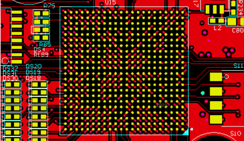
Electrical improvements include enhanced signal integrity and reduced EMI. Filled vias lower via stub inductance, supporting higher data rates in multilayer routing. They also enable tighter spacing for BGA escapes, maximizing real estate in dense designs. Overall, these benefits allow for thinner boards or fewer layers, optimizing cost without sacrificing performance.
Reliability in harsh environments further underscores their value. Filled vias resist moisture ingress, a common failure mode in unfilled structures exposed to humidity or cleaning agents. This aligns with factory-driven quality controls, ensuring boards meet stringent acceptance criteria.
Practical Solutions and Best Practices for Implementing Filled Vias
Selecting via filling materials depends on the application: use conductive epoxy for power vias needing parallel current paths, and non-conductive resin for signals to avoid capacitance changes. Consult laminate CTE data to match filler properties, ensuring compatibility across the stackup. In design, specify filled vias in netlists for critical nets, limiting their use to necessary locations to control costs.
Fabrication best practices include sequential filling post-plating, followed by planarization to maintain surface flatness. For high-layer-count builds, integrate filling during core lamination to avoid voids from high-aspect ratios. Test panels per IPC-TM-650 methods to verify fill density above 90 percent, confirming no air pockets via cross-sectioning. Engineers should collaborate with fabricators early, providing stackup details for aspect ratio feasibility.
In assembly, filled vias simplify solder paste printing by providing flat surfaces, reducing defects under BGAs. For high-reliability PCBs, qualify processes with thermal cycle testing to simulate field conditions. Avoid overfilling that could cause blowouts during reflow by controlling viscosity and cure profiles.
Case Insights from High-Reliability Applications
In server motherboards with 40-plus layers, filled vias have proven essential for maintaining interconnect integrity amid power plane demands. Designers report warpage reductions enabling reliable BGA attachment post-assembly. Similarly, in aerospace PCBs, non-conductive filled microvias prevent cracking in stacked configurations, supporting vibration resistance.
Conclusion
Filled vias represent a proven strategy for overcoming reliability hurdles in high-layer-count PCBs. By enhancing mechanical stability, thermal performance, and electrical characteristics, they enable denser, more robust designs. Via filling materials play a pivotal role in tailoring solutions to specific needs, from power to signal integrity. Electrical engineers benefit from incorporating them thoughtfully, guided by standards like IPC-4761 and IPC-6012. As electronics push boundaries, filled vias ensure high-reliability PCBs deliver consistent performance in demanding environments.
FAQs
Q1: What are PCB filled vias, and how do they differ from standard vias?
A1: PCB filled vias are through-holes or microvias completely filled with conductive or non-conductive materials after plating, unlike standard unfilled vias that retain an air gap. This filling eliminates voids, improving mechanical strength and preventing moisture entrapment. In high-layer-count boards, they reduce warpage from CTE mismatches. Factory processes ensure uniform fills for reliability.
Q2: What via filling materials are used for high-reliability PCBs?
A2: Common via filling materials include non-conductive epoxy resins for signal vias and conductive silver or copper epoxies for power applications. These materials match laminate CTE to minimize stress. Selection depends on thermal and electrical needs, with resins offering planar surfaces for assembly. They enhance overall PCB reliability without adding significant weight.
Q3: Why are filled vias beneficial in high-layer-count PCBs?
A3: Filled vias in high-layer-count PCBs boost thermal dissipation, lower inductance, and strengthen against thermal cycling failures. They enable higher routing density and tighter BGA pitches by maintaining board flatness. This supports high-reliability PCB requirements in multilayer stacks prone to warpage. Standards guide their implementation for consistent performance.
Q4: When should engineers specify filled vias in PCB designs?
A4: Specify filled vias for critical power or high-speed nets in boards exceeding 20 layers, especially with stacked microvias or fine-pitch components. They are ideal when warpage or reliability testing reveals issues with unfilled structures. Balance with cost by targeting high-risk areas. Collaboration with manufacturers ensures process compatibility.
References
IPC-4761 — Design Guide for Protection of Printed Board Via Structures. IPC, 2007
IPC-6012E — Qualification and Performance Specification for Rigid Printed Boards. IPC, 2017
IPC-A-600K — Acceptability of Printed Boards. IPC, 2020