Introduction
In printed circuit board manufacturing, the choice of minimum drill size plays a critical role in determining overall pcb drill size reliability. Smaller holes enable denser designs but introduce risks during drilling and plating processes that can compromise long-term performance. Engineers must balance design density with manufacturability to prevent defects like drill wander and inadequate plating. This article explores how minimum drill size influences DFM considerations and highlights strategies to maintain structural integrity. By understanding these factors, designers can enhance pcb hole plating issues mitigation and meet annular ring requirements effectively. Factory insights reveal that proactive DFM checks significantly reduce yield losses in high-volume production.
Understanding Minimum Drill Size and Its Relevance to PCB Reliability
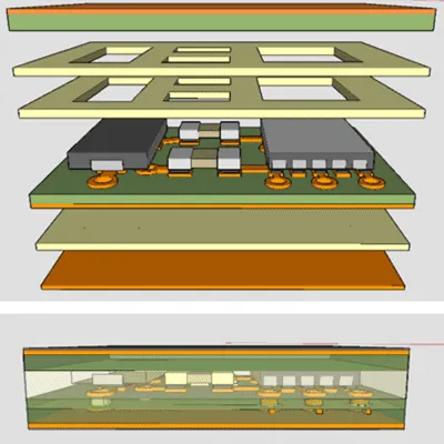
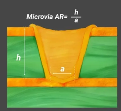
Minimum drill size refers to the smallest diameter achievable for vias or through-holes in a PCB stackup, constrained by mechanical or laser drilling capabilities. In standard processes, mechanical drilling sets practical limits based on bit rigidity and board thickness, while laser drilling allows finer features but at higher costs. Pcb drill size reliability directly affects signal integrity, thermal management, and mechanical strength, as undersized holes amplify process variations. For instance, high aspect ratios from small drills challenge plating uniformity, leading to voids or cracks under thermal stress. Industry standards like IPC-6012 outline performance criteria that indirectly guide drill size selection through plating and hole wall quality requirements. Neglecting these can result in field failures, underscoring the need for DFM integration early in design.
Designers often overlook how minimum drill size dfm impacts yield during fabrication. Factories prioritize aspect ratios, typically board thickness to hole diameter, to ensure reliable plating chemistry flow. Exceeding recommended ratios increases defect rates, as electrolyte penetration becomes uneven. Reliability testing, including thermal cycling, exposes weaknesses in small-hole barrels more readily than larger ones. Electrical engineers should collaborate with manufacturers to align designs with proven capabilities, avoiding costly respins. This factory-driven approach ensures consistent performance across production runs.
Mechanisms of Drill Wander in PCB Manufacturing
Drill wander pcb occurs when the drill bit deviates from its intended path, primarily due to bit deflection under lateral forces during penetration. Smaller diameter bits, being less rigid, amplify this effect, especially in thicker boards or dense via fields. The phenomenon worsens with entry and exit breakthrough, where material inconsistencies cause erratic motion. Resulting misalignment reduces effective annular ring width, risking copper breakout and open circuits. Factories mitigate this through peck drilling cycles and optimized feed rates, but design margins remain essential for reliability.
Material properties exacerbate drill wander. Fiberglass reinforcement in laminates creates anisotropic resistance, steering thin bits off-axis. High-speed spindles help, yet wander persists below certain diameters, correlating with increased scrap rates. Post-drill inspection via automated optical systems detects offsets, but prevention trumps correction in DFM. Engineers can model wander risks using fabrication tolerances to set conservative drill sizes. Consistent entry-exit material preparation further stabilizes the process.
In multilayer boards, sequential drilling compounds wander across layers, misaligning inner vias. Registration errors propagate, threatening interlayer connections. Standards like IPC-A-600 define acceptability for hole location, emphasizing the need for robust drill size choices. By simulating stackup dynamics, designers predict and avert these issues proactively.
PCB Hole Plating Challenges with Minimum Drill Sizes
Pcb hole plating issues arise prominently with small drill sizes due to limited electrolyte access in high-aspect-ratio holes. Plating chemistry must uniformly deposit copper on hole walls, but capillary forces hinder flow in narrow barrels. This leads to plating voids, thin spots, or separation under thermal expansion. Reliability suffers as microcracks form during reflow or operation, accelerating failure in high-frequency applications.
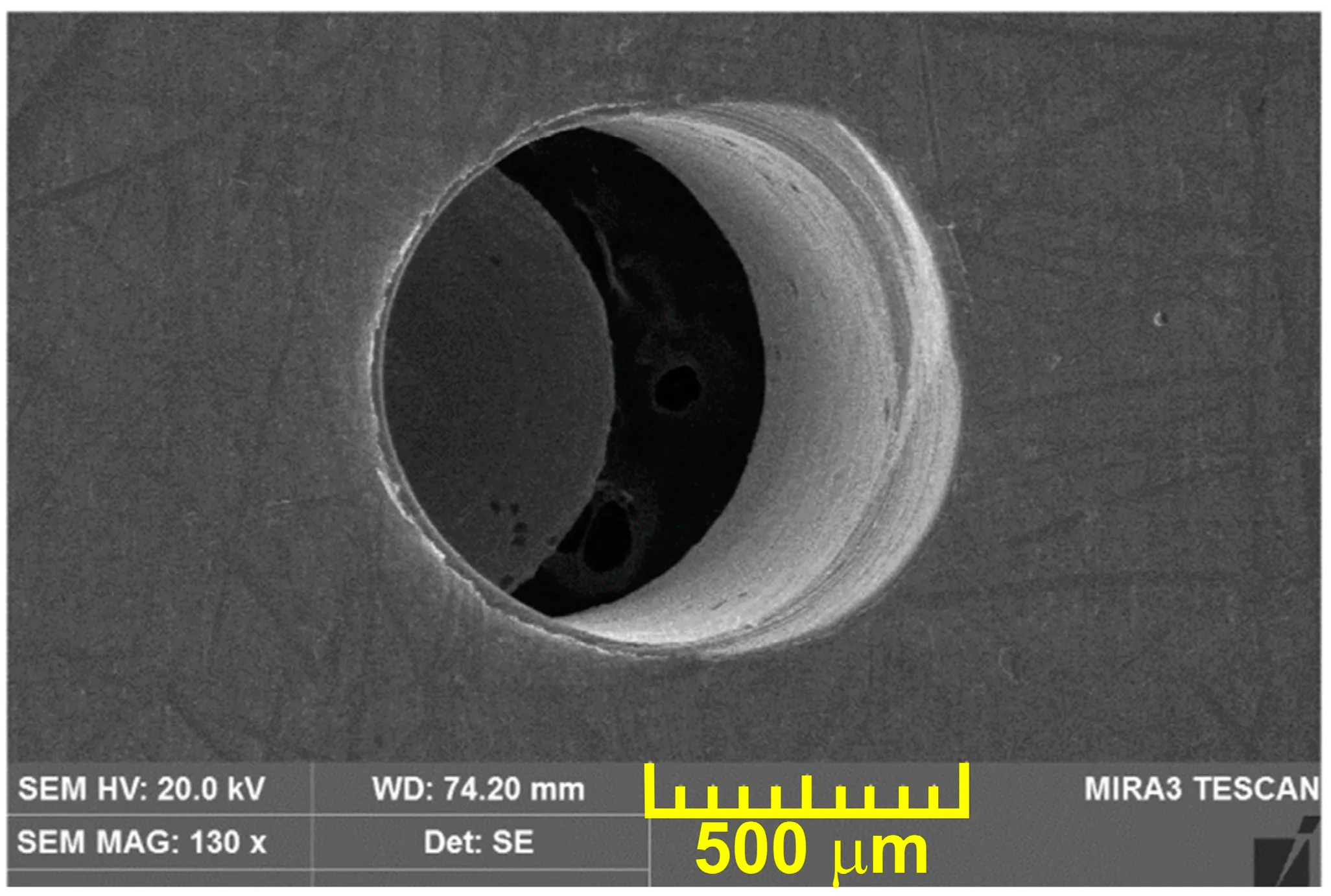
Desmear processes precondition holes by removing resin smear from drilling, but aggressive chemistries etch walls unevenly in small diameters. Residual smear traps air, promoting voids during electroplating. Factories employ pulse plating or vacuum assistance for better coverage, yet design aspect ratios dictate feasibility. Exceeding limits invites barrel cracks, detectable via cross-section analysis.
Plating thickness uniformity ties directly to current distribution, favoring outer layers over deep interiors. Small holes intensify edge effects, thinning inner copper. IPC-6012 specifies minimum barrel wall thickness for performance classes, guiding DFM rules. Engineers mitigate by oversizing drills where density allows, prioritizing reliability over minimalism.
Annular Ring Requirements in Relation to Drill Size DFM
Annular ring requirements ensure sufficient copper surrounds plated holes, preventing breakout and supporting solder joints. Minimum drill size dfm directly influences ring adequacy, as wander or plating buildup erodes margins. External layers demand larger rings for mechanical robustness, while internals tolerate slivers under standards. IPC-2221 provides design guidelines for ring dimensions based on fabrication levels, stressing drill-to-copper clearances.
Breakout occurs when drill wander encroaches on pads, especially in blind vias. Factories measure rings post-plating, rejecting boards below class thresholds. Dense via grids compound risks, as anti-pad sizing competes with trace spacing. DFM tools flag violations by incorporating positional tolerances.
Optimal annular rings enhance thermal dissipation and vibration resistance. Undersized rings crack under cyclic loads, compromising pcb drill size reliability. Designers allocate 10-20% extra pad area for small drills, verified through fab feedback loops. This balances density with manufacturability.
Best Practices for Selecting Minimum Drill Sizes in DFM
Adopt conservative aspect ratios, ideally under 10:1, to safeguard plating integrity and minimize drill wander pcb risks. Collaborate with fabricators for capability matrices outlining viable drill sizes per stackup. Incorporate drill-to-copper minimums in layout rules, ensuring annular ring compliance across classes.
Leverage simulation for plating flow and stress analysis on small holes. Peck drilling and backup materials reduce wander in production. Post-drill deburring prevents plating defects from debris.
Specify class-appropriate tolerances in fab drawings, referencing IPC standards. Prototype high-risk designs to validate reliability under accelerated life tests. Iterative DFM reviews catch issues early.
Troubleshooting Common Manufacturing Defects
Factories encounter drill breakout from wander in 5-10% of small-hole runs without margins. Cross-sections reveal slivered rings; remedy via larger drills or laser alternatives. Plating voids manifest as high-resistance vias; etch-back optimization resolves most.
Annular ring shortfalls trigger electrical opens; redesign pads with breakout allowances per IPC-A-600. Yield data guides future specs, emphasizing minimum drill size dfm.
Conclusion
Minimum drill size profoundly impacts pcb drill size reliability through interconnected effects on drilling accuracy, plating quality, and annular ring integrity. Prioritizing DFM principles averts defects like drill wander and hole wall failures. Engineers achieve robust designs by aligning with standards and fab capabilities. Proactive strategies ensure high yields and field durability. Invest in these practices for sustained performance.
FAQs
Q1: What role does minimum drill size play in pcb drill size reliability?
A1: Minimum drill size affects reliability by influencing plating uniformity and mechanical stability. Small diameters heighten drill wander risks and aspect ratio challenges, potentially causing voids or cracks. Adhering to fab capabilities and standards like IPC-6012 maintains integrity. Factory experience shows balanced sizing boosts long-term performance.
Q2: How does drill wander pcb impact manufacturing yields?
A2: Drill wander deviates bits in small holes, eroding annular rings and causing breakouts. Thinner bits deflect more in reinforced materials, amplifying defects. Peck cycles and margins mitigate this. Dfm checks prevent yield drops in dense designs.
Q3: Why are pcb hole plating issues common with small minimum drill sizes?
A3: Small drills create high-aspect holes restricting electrolyte flow, leading to thin or voided plating. Desmear inconsistencies exacerbate this. Standards guide maximum ratios for coverage. Oversizing where possible enhances reliability.
Q4: What are key annular ring requirements for minimum drill size dfm?
A4: Annular rings must surround holes adequately per IPC guidelines, varying by layer and class. Small drills demand extra pad margins to counter wander. Fab tolerances ensure compliance. Proper sizing avoids electrical and mechanical failures.
References
IPC-6012E — Qualification and Performance Specification for Rigid Printed Boards. IPC, 2017
IPC-A-600K — Acceptability of Printed Boards. IPC, 2020
IPC-2221B — Generic Standard on Printed Board Design. IPC, 2012