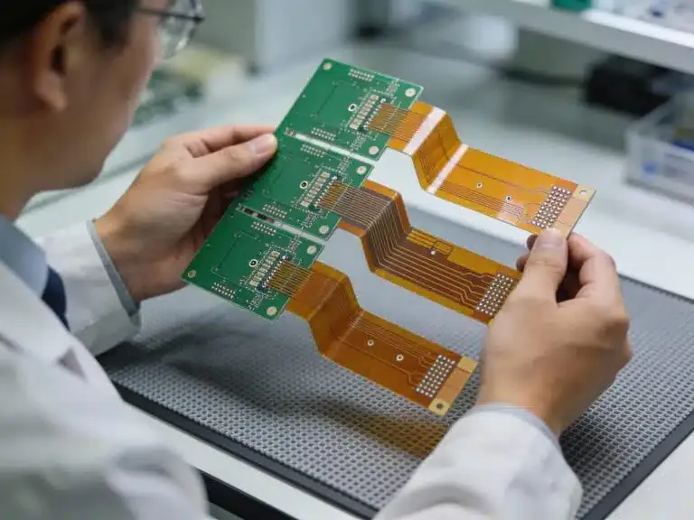
Introduction
Pad-to-pad spacing represents a critical parameter in PCB design that directly influences thermal performance, particularly in applications demanding efficient pcb thermal management. As electronic devices incorporate higher power densities, components generate more heat, making optimal spacing essential to prevent hotspots and ensure reliability. Insufficient spacing can restrict heat spreading paths, while excessive gaps may underutilize board real estate. Engineers must balance manufacturability, electrical isolation, and thermal dissipation when defining pad layouts. This article explores the mechanisms, best practices, and design considerations for leveraging pad spacing to enhance heat dissipation pad spacing and support high power component placement. By understanding these relationships, designers can achieve superior thermal via design and overall board performance.
Understanding Pad-to-Pad Spacing in PCB Thermal Management
Pad-to-pad spacing refers to the minimum distance between the edges of adjacent conductive pads on a PCB surface, governed by standards like IPC-2221 for generic printed board design. This spacing ensures electrical clearance, solder mask application, and assembly feasibility, but it also plays a pivotal role in pcb thermal management by dictating the availability of copper areas for heat conduction. In densely populated boards, tight spacing limits the width of copper pours or planes that act as heat spreaders, potentially increasing thermal resistance between components. Conversely, adequate spacing allows for broader copper interconnects that facilitate lateral heat flow across the board. For high power component placement, such as power ICs or regulators, engineers prioritize spacing to accommodate thermal relief pad benefits, which mitigate soldering challenges without compromising operational heat transfer. Ultimately, spacing decisions impact the entire thermal pathway, from component junction to ambient environment.
The Physics of Heat Dissipation and Pad Spacing Effects
Heat dissipation in PCBs primarily occurs through conduction via copper traces, pads, and planes, with pad-to-pad spacing modulating the effective cross-sectional area for this transfer. When pads are closely spaced, the intervening copper region narrows, elevating thermal impedance and causing localized temperature rises, especially under high power component placement. This constriction forces more reliance on vertical heat paths via thermal vias, which may become congested in tight layouts. Broader spacing enables expansive copper flooding, promoting uniform heat spreading and reducing peak temperatures by distributing thermal loads. Convection and radiation contribute marginally at the board level, but optimized spacing enhances their effectiveness by lowering surface temperatures. According to IPC-2221 guidelines, spacing must account for these thermal dynamics alongside electrical requirements to maintain board integrity under load.
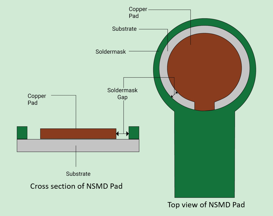
Role of Thermal Relief Pads in Balancing Assembly and Performance
Thermal relief pads introduce intentional gaps or spokes between component pads and large copper areas, offering thermal relief pad benefits during reflow soldering by reducing heat sinking. This design prevents rapid heat loss from the solder joint, ensuring proper melting and formation without defects. However, in operational pcb thermal management, these reliefs slightly increase thermal resistance compared to solid connections, as the spokes limit direct conduction paths. For heat dissipation pad spacing, engineers must evaluate relief geometry alongside adjacent pad distances to avoid compounding thermal bottlenecks. In high power applications, minimizing relief spoke width or opting for full copper under non-pinned thermal pads optimizes runtime performance. The interplay requires simulation or empirical validation to quantify impacts on junction temperatures.
Integrating Thermal Vias with Pad Spacing Strategies
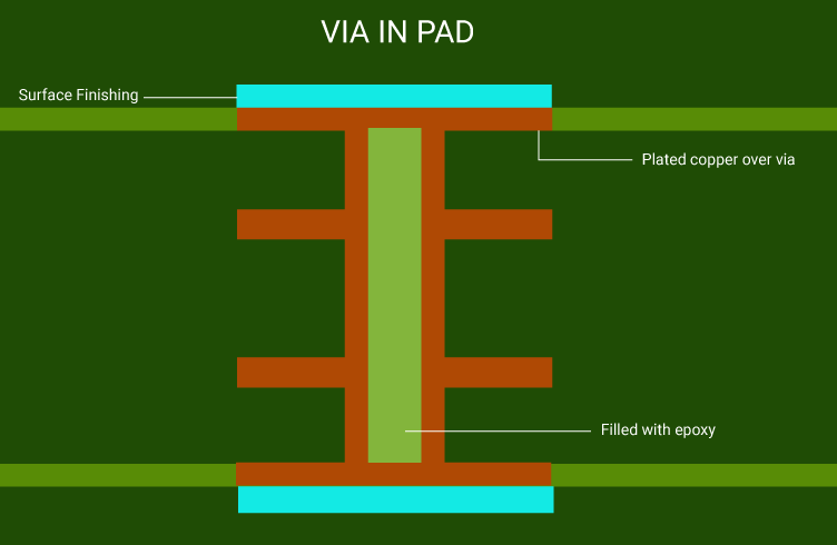
Thermal via design becomes indispensable when pad-to-pad spacing constrains surface-level heat spreading, channeling heat to inner layers or ground planes efficiently. Vias placed between or around pads transfer heat vertically, but their positioning demands sufficient spacing to avoid solder wicking or shorting during assembly. Optimal heat dissipation pad spacing accommodates via arrays without encroaching on pad margins, typically aligning with IPC class definitions for drill-to-pad clearances. For high power component placement, via-in-pad techniques under exposed thermal pads enhance dissipation, provided surrounding pad spacing permits mask-defined land patterns. Arrays of vias with staggered patterns maximize coverage while respecting spacing minima, reducing via thermal resistance collectively. Designers iterate layouts to ensure vias do not cluster excessively, preserving board structural integrity.
Best Practices for High Power Component Placement and Spacing Optimization
Start with component libraries adhering to land pattern standards to establish baseline pad sizes and spacings suited for thermal demands. Increase pad-to-pad spacing around high power devices by 20 to 50 percent beyond electrical minima where feasible, prioritizing copper pour continuity for lateral spreading. Employ ground or power planes on multiple layers, connected via thermal vias arrays tailored to spacing allowances. For thermal relief pad benefits in mixed-signal boards, use 90-degree spoke patterns to balance assembly and conduction. Validate designs through thermal modeling, adjusting spacing iteratively to meet junction temperature targets. Document spacing rationales per layer to facilitate fabrication reviews.
Advanced Considerations: Layer Stackup and Material Interactions
Multilayer boards amplify spacing benefits, as inner layers provide uninterrupted planes decoupled from surface pad constraints. Copper thickness influences effective spacing utility; thicker foils enhance conduction across gaps. Material choices, like high-Tg laminates, support tighter spacings under thermal stress without delamination. High power component placement near board edges leverages natural convection, allowing marginally reduced spacings. Simulate airflow over spaced pads to predict forced convection enhancements. Adhere to performance specs like IPC-6012 for qualification under thermal cycling.
Case Insights: Optimizing for Power Converters
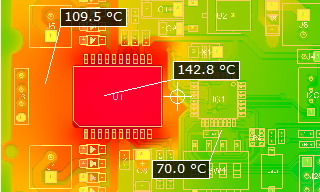
In a typical DC-DC converter design, initial tight pad spacing around the inductor and MOSFETs resulted in elevated die temperatures during full load. Expanding spacing by reallocating non-critical traces enabled a full copper pour and additional thermal vias, dropping hotspot deltas by noticeable margins. Thermal relief pads on control IC pins maintained assembly yields while solid pads under power devices boosted dissipation. This adjustment aligned with high power component placement needs, demonstrating spacing's leverage on overall pcb thermal management. Post-prototype infrared imaging confirmed uniform profiles. Such refinements underscore iterative design's value.
Conclusion
Pad-to-pad spacing profoundly shapes PCB thermal performance by governing heat spreading capacity, via integration, and relief trade-offs. Strategic increases around high power areas, coupled with robust thermal via design, yield resilient pcb thermal management solutions. Adhering to standards like IPC-2221 ensures manufacturability without thermal penalties. Engineers gain most by simulating interactions early, balancing density with dissipation. Implementing these principles elevates board reliability in demanding applications, from power supplies to RF modules.
FAQs
Q1: How does heat dissipation pad spacing affect high power component placement?
A1: Heat dissipation pad spacing directly influences the copper area available for lateral conduction around high power components. Wider spacing reduces thermal resistance by enabling broader pours and via placement, preventing hotspots. Tight layouts force vertical paths, increasing reliance on inner layers. Optimize by prioritizing power devices with extra margins while respecting IPC minima. This approach enhances overall junction-to-ambient transfer in pcb thermal management.
Q2: What are the thermal relief pad benefits in pcb thermal management?
A2: Thermal relief pad benefits include easier reflow soldering by limiting heat sinking from large coppers, reducing defects like incomplete joints. Spokes confine heat to the pad, aiding assembly yields. Operationally, they introduce minor resistance increases, balanced by surrounding spacing. Use judiciously for high power pins, favoring solid connections elsewhere. Integration supports reliable heat dissipation pad spacing strategies.
Q3: Why is thermal via design critical with constrained pad spacing?
A3: Thermal via design compensates for limited surface spreading in tight pad spacing by routing heat to planes efficiently. Arrays under or adjacent to pads lower resistance, with spacing dictating via density. Avoid wicking by tenting unused vias and aligning with pad margins. This elevates pcb thermal management for high power component placement. Proper arrays can equalize temperatures across layers.
Q4: How to optimize pad-to-pad spacing for better thermal performance?
A4: Optimize pad-to-pad spacing by starting with standard clearances, then expanding for power zones to fit copper floods and vias. Model thermal paths to quantify gains from incremental increases. Balance with density needs, using multilayer planes for support. This refines heat dissipation pad spacing, aligning with high power component placement goals in pcb thermal management.
References
IPC-2221B — Generic Standard on Printed Board Design. IPC, 2003
IPC-6012E — Qualification and Performance Specification for Rigid Printed Boards. IPC, 2015