Introduction
Printed circuit boards serve as the foundation for electronic systems, where thermal management directly impacts reliability and performance. PCB thickness plays a critical role in how effectively heat generated by components dissipates across the board. Engineers must balance mechanical stability with thermal conductivity when selecting thickness, as suboptimal choices lead to hotspots, reduced lifespan, or assembly failures. This guide explores the interplay between PCB thickness and thermal resistance, highlighting practical considerations for design and manufacturing. By understanding these dynamics, electric engineers can optimize designs for demanding applications.
Understanding PCB Thickness and Its Thermal Relevance
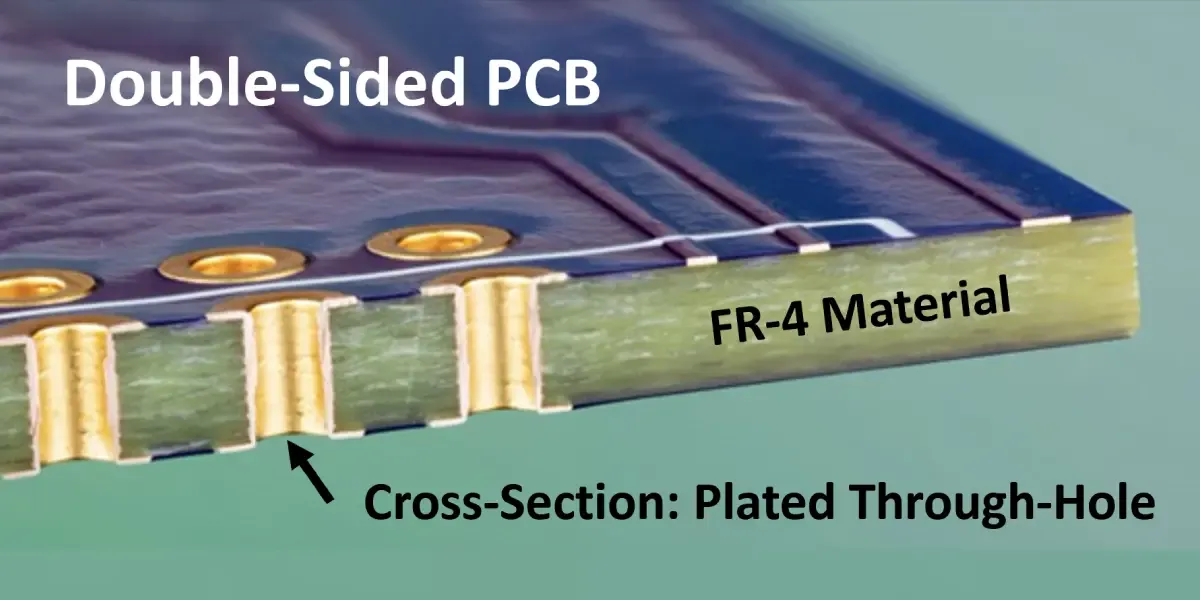
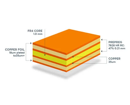
PCB thickness refers to the total height of the board stackup, encompassing copper layers, dielectrics, and prepregs. Standard thicknesses vary based on application needs, influencing both electrical and thermal properties. Thinner boards offer flexibility in compact designs but introduce specific thermal challenges, while thicker ones provide robustness. Thermal management hinges on how thickness affects heat paths, from vertical conduction through dielectrics to lateral spreading via copper planes. Engineers evaluate PCB thickness and thermal resistance early to prevent issues like component overheating.
In high-power electronics, PCB thickness determines the board's ability to act as a heat spreader. Thicker constructions enhance mechanical integrity, supporting heavier components and reducing flexing under thermal cycling. However, the dielectric portion of the stackup dominates thermal resistance in the through-plane direction. As thickness increases, the path length for heat transfer lengthens, potentially elevating junction temperatures. This relationship underscores the need for simulations during the design phase.
Technical Principles of PCB Thickness and Thermal Resistance
Heat flow in PCBs follows Fourier's law, where thermal resistance inversely relates to conductivity and cross-sectional area but directly to path length. PCB thickness and thermal resistance correlate closely, with thicker dielectrics impeding vertical heat transfer due to materials like FR-4 having low through-plane conductivity. Copper layers, despite high in-plane conductivity, contribute minimally if dielectric gaps widen. Engineers model effective thermal conductivity considering layer thicknesses and fill factors. This principle guides stackup decisions for uniform temperature distribution.
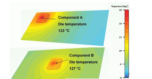
Lateral heat spreading benefits from copper plane dimensions rather than total thickness alone, yet board rigidity from added layers aids overall dissipation. Thicker PCB for heat dissipation proves advantageous in scenarios requiring structural support for heatsinks or enclosures. Conversely, excessive thickness raises impedance to heat sinking on the opposite side. Finite element analysis reveals hotspots forming near high-power devices if thickness mismatches thermal loads. IPC-2221 outlines design guidelines for such thermal management aspects, emphasizing balanced stackups.
Thin PCB Thermal Challenges
Thin PCBs, often under 1 mm, excel in space-constrained applications like wearables or high-density interconnects. However, thin PCB thermal challenges arise from limited dielectric volume and heightened sensitivity to imbalances. Reduced rigidity amplifies warpage under thermal stress, misaligning components during reflow. Heat concentrates in narrow paths, exacerbating hotspots without adequate spreading area. Moisture absorption worsens these effects, as thinner boards desorb slower during heating.
Assembly processes intensify issues, with non-uniform reflow profiles causing differential expansion. Thin substrates struggle to distribute stress from coefficient of thermal expansion mismatches between copper and resin. This leads to delamination risks or solder joint failures. Designers mitigate by incorporating thermal vias, though their efficacy diminishes in ultra-thin builds. JEDEC standards like J-STD-020 address reflow sensitivity, indirectly influencing thickness choices for thermal stability.
Related Reading: Enhancing PCB Reliability: A Guide to Thermal Vias for Heat Dissipation
Advantages of Thicker PCBs for Heat Dissipation
Thicker PCB for heat dissipation offers superior mechanical stability, minimizing deflection under load. Increased mass provides a larger thermal reservoir, smoothing temperature spikes from pulsed operation. Robustness allows secure mounting of large heatsinks, enhancing convection and radiation. Copper-to-dielectric ratios improve in multi-layer thick boards, boosting effective in-plane conductivity. Applications in power supplies or automotive electronics favor this approach for sustained performance.
While through-plane resistance rises slightly, overall system-level dissipation improves via better interface contacts. Thicker boards resist deformation, ensuring consistent via thermal performance. Fabrication yields stabilize as warpage risks drop. Engineers select thicknesses aligning with enclosure constraints and airflow paths. Practical testing confirms lower peak temperatures compared to thin alternatives under equivalent power.
Related Reading: Solving Thermal Challenges in PCB Prototyping: Techniques for Heat Dissipation
Optimal PCB Thickness for Thermal Performance
Optimal PCB thickness for thermal performance emerges from trade-offs between conduction paths, rigidity, and manufacturing feasibility. Simulations using finite element methods predict temperature profiles across candidate stackups. Factors include power density, ambient conditions, and cooling methods. Typically, designs converge on thicknesses balancing dielectric gaps for interlayer heat transfer with overall stiffness. Iterative prototyping refines choices, validating models against real-world operation.
Layer count influences outcomes, as inner planes add parallel thermal paths despite total height increase. Copper weight selection complements thickness, with heavier foils aiding spreading. Board warpage thermal considerations demand symmetric stackups to equalize expansion. IPC-A-600 specifies acceptability criteria for flatness, guiding thickness-related decisions. Comprehensive design reviews integrate these elements for peak efficiency.
Board Warpage and Thermal Considerations
Board warpage thermal considerations stem from mismatched coefficients of thermal expansion during lamination and assembly. Thinner boards warp more readily as stress concentrates without damping from bulk material. Asymmetric copper distribution exacerbates bowing, altering heat flow paths post-fabrication. Reflow soldering amplifies curvature, risking BGA voids or tombstoning. Pre-bake and controlled ramps mitigate but cannot fully compensate poor stackup symmetry.
Thicker constructions inherently resist warpage, distributing thermal strains evenly. Fixturing during assembly preserves flatness for precision placement. Material selection with matched CTEs further stabilizes boards. Long-term reliability testing cycles reveal warpage evolution under operational thermals. Engineers prioritize bow and twist limits per industry benchmarks to safeguard thermal integrity.
Best Practices for Selecting and Implementing PCB Thickness
Begin with power budget analysis to estimate heat loads per component. Model stackups varying thickness, incorporating via fields and plane cuts for vias. Collaborate with fabricators early on tolerances and material options. Prototype high-risk designs to measure real thermal profiles using thermocouples or IR imaging. Incorporate redundancy like embedded heat pipes for extreme cases.
Symmetric layering prevents warpage, with core and prepreg thicknesses mirrored. Thermal vias under hotspots bridge layers effectively, sized per conduction needs. Surface finishes influence contact resistance to sinks. Post-assembly bake stabilizes boards against humidity-induced shifts. Documentation of rationale ensures repeatability across revisions.
Conclusion
PCB thickness profoundly shapes thermal management outcomes, from resistance profiles to warpage resilience. Thicker designs excel in dissipation and stability for power-intensive uses, while thin variants demand careful mitigation of vulnerabilities. Optimal choices integrate simulations, standards, and testing for balanced performance. Electric engineers achieve reliable systems by prioritizing these factors throughout the design cycle. Future advancements in materials will further refine thickness selections, enhancing overall efficiency.
FAQs
Q1: What is the relationship between PCB thickness and thermal resistance?
A1: PCB thickness and thermal resistance increase together primarily due to longer dielectric paths impeding through-plane conduction. Thicker boards raise vertical resistance but improve lateral spreading capacity via added layers. Engineers model this using effective conductivity values, adjusting for copper fill. Proper stackup symmetry ensures minimal hotspots, aligning with design standards for thermal performance.
Q2: When should a thicker PCB be used for heat dissipation?
A2: Opt for thicker PCB for heat dissipation in high-power applications needing mechanical support and larger thermal mass. It resists warpage under cycling and facilitates heatsink attachment. Balance with simulations to avoid excess through-plane resistance. This approach suits power electronics where stability trumps minimal height.
Q3: What are common thin PCB thermal challenges?
A3: Thin PCB thermal challenges include pronounced warpage from CTE mismatches and limited heat spreading area. Hotspots form rapidly without robust planes, risking component failure during reflow. Moisture sensitivity heightens delamination risks. Mitigate with vias, symmetric designs, and controlled profiles for reliable operation.
Q4: How does board warpage affect thermal considerations in PCB thickness selection?
A4: Board warpage thermal considerations demand thicker or symmetric stackups to distribute stress evenly. Warped boards disrupt heat paths and assembly alignment, elevating resistances. Standards limit bow and twist to preserve performance. Testing under thermal loads validates choices for long-term stability.
References
IPC-2221 — Generic Standard on Printed Board Design. IPC, 2012
IPC-A-600K — Acceptability of Printed Boards. IPC, 2020
J-STD-020E — Moisture/Reflow Sensitivity Classification for Nonhermetic Surface Mount Devices. JEDEC, 2014