Introduction
Copper thickness plays a critical role in PCB design, influencing everything from current-carrying capacity to signal integrity and thermal performance. Engineers often encounter specifications in ounces per square foot (oz/ft2), a weight-based unit rooted in copper foil manufacturing traditions. However, many design tools and simulations require direct thickness measurements in mils, leading to the need for reliable copper thickness conversion between these units. This article provides the ultimate mils to ounces converter, complete with charts, formulas, and practical guidance tailored for electric engineers. By mastering PCB units conversion, designers can avoid costly errors in prototyping and production. Whether optimizing trace widths or selecting foil weights, understanding these relationships ensures robust board performance.
Why Copper Thickness Matters in PCB Design
Copper thickness directly determines a trace's ability to handle current without excessive heating, as thicker copper reduces resistance and improves heat dissipation. In high-power applications, insufficient thickness leads to voltage drops, electromigration, and potential board failure under load. Conversely, overly thick copper increases material costs, complicates etching, and raises impedance mismatches in high-frequency signals. Industry standards like IPC-6012 define minimum finished copper thicknesses to ensure reliability across manufacturing variations. For multilayer boards, balancing inner and outer layer thicknesses affects overall stackup integrity and via performance. Accurate copper thickness conversion becomes essential when collaborating across teams using different units, preventing miscommunications that delay projects.
Signal integrity engineers rely on precise mils values for modeling skin effect and insertion loss, where even small deviations alter high-speed performance. Procurement teams benefit from copper weight charts to evaluate cost implications during quoting. Ultimately, proper PCB units conversion streamlines the design-to-fabrication workflow, aligning specifications with manufacturing capabilities.
Understanding Copper Thickness Units and Their Origins
The ounce per square foot unit originates from the process of rolling copper foil: one ounce of copper spread evenly over one square foot yields a nominal thickness of 1.37 mils. This convention persists because it simplifies specifying foil weights before etching and plating. Mils, or thousandths of an inch, provide a linear measure ideal for CAD tools and cross-section analysis. The conversion factor derives from copper's density of approximately 8.96 g/cm3, with 1 oz/ft2 equating to 35 μm or 1.37 mils exactly. Variations occur due to electrodeposition or electrodeposited foils, but nominal values guide design. Engineers must distinguish base foil thickness from finished thickness after processing, as plating adds 0.2-1 mil depending on requirements.
In practice, 1 oz/ft2 base copper becomes about 1.2-1.4 mils finished on outer layers per IPC-6012 guidelines. Inner layers typically retain closer to nominal due to less plating. Microns offer a metric alternative, with 1 mil equaling 25.4 μm, facilitating global collaboration. A simple formula for conversion is: thickness (mils) = copper weight (oz/ft2) × 1.37. This relationship holds for standard rolled annealed (RA) or electrodeposited (ED) foils used in most PCBs.
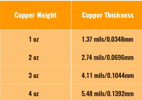
The Ultimate Copper Thickness Conversion Chart
For quick reference, the following list compiles standard PCB copper weights with equivalent thicknesses in mils, microns, and grams per square meter. These values represent nominal base foil thicknesses before fabrication losses.
- 0.25 oz/ft2 — 0.34 mils — 8.9 μm — 76 g/m2
- 0.5 oz/ft2 — 0.69 mils — 17.5 μm — 152 g/m2
- 1.0 oz/ft2 — 1.37 mils — 35 μm — 305 g/m2
- 1.5 oz/ft2 — 2.06 mils — 52.5 μm — 457 g/m2
- 2.0 oz/ft2 — 2.74 mils — 70 μm — 610 g/m2
- 3.0 oz/ft2 — 4.11 mils — 105 μm — 915 g/m2
- 4.0 oz/ft2 — 5.48 mils — 140 μm — 1220 g/m2
- 5.0 oz/ft2 — 6.85 mils — 175 μm — 1525 g/m2
- 6.0 oz/ft2 — 8.22 mils — 210 μm — 1830 g/m2
This copper weight chart accounts for industry norms, where 1 oz and 2 oz dominate standard designs. For heavy copper PCBs exceeding 3 oz/ft2, expect adjusted etching factors and higher minimum trace widths. Use this as a PCB calculator starting point, verifying with vendor capabilities.
Technical Principles of Copper Thickness in PCB Fabrication
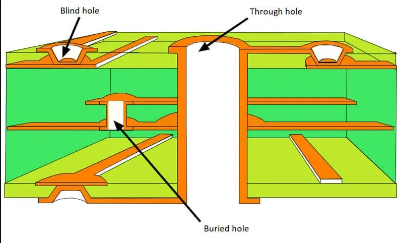
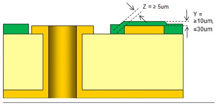
During lamination, base copper foil bonds to the dielectric core, with outer layers often plated to compensate for etching losses. IPC-A-600 specifies acceptability criteria, requiring minimum finished thicknesses like 0.9 mil for 1 oz outer layers and 1.2 mil for 2 oz. Plating viax or panels adds copper uniformly, but uneven current density can cause variations up to 20%. Reverse treated foil (RTF) improves adhesion and uniformity compared to standard ED foil. Thickness uniformity impacts impedance control, as dielectric height relative to copper affects characteristic impedance formulas. Engineers calculate effective thickness using stackup models incorporating these tolerances.
Skin effect at high frequencies confines current to the outer copper surface, making effective thickness roughly 2 mils at 1 GHz for 1 oz copper. This principle underscores why heavier copper benefits RF designs despite higher losses. Thermal expansion mismatches between copper and FR-4 can induce warpage if thicknesses are imbalanced across layers.
Practical Best Practices for Copper Thickness Selection
Start with 1 oz/ft2 for most signal layers to balance cost and performance, escalating to 2 oz for power traces exceeding 3A. Use IPC-2221 trace width charts, inputting mils thickness from your conversion to size conductors for desired temperature rise. For high-current designs, employ a mils to ounces converter formula iteratively with simulation tools. Specify finished copper requirements in fab drawings to account for 10-20% etchback. In multilayer stackups, heavier inner layers aid heat spreading but demand wider traces to prevent shorts. Always prototype and measure cross-sections to validate conversions against actual boards.
Validate designs with thermal simulations incorporating real thickness data. For flex or rigid-flex PCBs, thinner copper like 0.5 oz minimizes bending stress. Document units clearly in gerbers and notes to avoid fab errors.
Troubleshooting Common Copper Thickness Issues
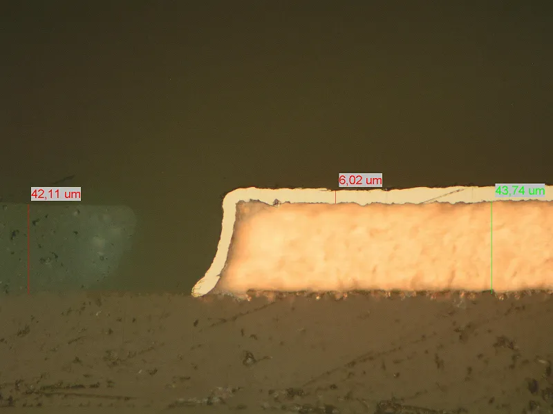
Designers frequently overlook plating shrinkage, resulting in traces thinner than calculated, leading to hotspots. Measure via microsectioning per IPC standards to confirm thicknesses post-fab. If impedance deviates, check copper roughness adding effective thickness. Overly thick copper causes under-etching, bridging fine-pitch features; compensate with adjusted artwork shrink factors. In high-density interconnects, verify HDI plating meets J-STD specs for via fill.
Uneven plating from poor rack design manifests as thickness gradients; request panel plating for uniformity. For heavy copper, ensure drill aspect ratios stay below 10:1 to maintain via integrity.
Conclusion
Mastering copper thickness conversion equips engineers with the precision needed for reliable PCB designs. The provided charts and formulas serve as an indispensable PCB calculator for daily workflows. Adhering to standards ensures manufacturability while optimizing electrical and thermal performance. Integrate these insights into your process to reduce iterations and enhance board quality. With accurate mils to ounces conversions, transition seamlessly from concept to production.
FAQs
Q1: How do I use a mils to ounces converter for PCB trace width calculations?
A1: Convert your desired oz/ft2 to mils using the factor 1.37, then input into IPC-2221-based calculators. For a 2 oz layer at 2.74 mils, a 20 mil wide trace handles about 10A with 20°C rise. Always factor in temperature and verify with simulations for safety margins. This PCB units conversion prevents undersized conductors in power designs.
Q2: What is the standard copper thickness for high-current PCB applications?
A2: Typically 2-3 oz/ft2, equating to 2.74-4.11 mils, to support currents over 5A without excessive heating. Reference copper weight charts for precise values and adjust trace widths accordingly. IPC guidelines mandate minimum finished thicknesses post-plating. Balance with cost and etchability for optimal results.
Q3: Can I create a custom copper thickness conversion chart for my PCB calculator?
A3: Yes, extend the standard table linearly: mils = oz × 1.37. Include tolerances like ±10% for fabrication. This aids quick PCB units conversion during stackup planning. Validate against measured cross-sections for accuracy.
Q4: Why does finished copper thickness differ from base foil in copper thickness conversion?
A4: Etching removes 15-25% of copper, offset by plating to meet specs like 1.37 mils nominal for 1 oz. IPC-6012 details minimums: 0.9 mil outer, 1.0 mil inner. Use copper weight charts adjusted for process losses.
References
IPC-6012E — Qualification and Performance Specification for Rigid Printed Boards. IPC, 2017
IPC-A-600K — Acceptability of Printed Boards. IPC, 2020
IPC-2221B — Generic Standard on Printed Board Design. IPC, 2012
J-STD-001H — Requirements for Soldered Electrical and Electronic Assemblies. IPC, 2018