Introduction
Designing a printed circuit board can seem daunting for beginners, but understanding key elements like copper thickness can make the process manageable. This guide focuses on 2oz copper PCB design, a popular choice for applications requiring higher current capacity and better heat dissipation. Aimed at electronic hobbyists, this 2oz copper PCB tutorial will walk you through essential concepts, practical tips, and industry standards. Whether you are working on a personal project or learning the ropes of PCB design, this beginner PCB design resource offers clear, structured insights. By following this easy PCB design approach, you will gain the confidence to create reliable and efficient boards tailored to your needs.
What Is 2oz Copper PCB and Why It Matters
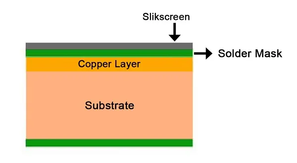
Copper thickness in a PCB is measured in ounces per square foot, indicating the weight of copper on the board's surface. A 2oz copper PCB means there are two ounces of copper per square foot, roughly translating to a thickness of about 2.8 mils or 70 micrometers. This is thicker than the standard 1oz copper, which is often used in basic designs. The increased thickness of 2oz copper allows for greater current carrying capacity and improved thermal management, making it ideal for power electronics, automotive circuits, and high performance hobbyist projects.
Why does this matter for beginners? Thicker copper reduces the risk of overheating and trace damage in circuits with higher current demands. It also enhances the durability of the board under mechanical stress. For hobbyists experimenting with power supplies or motor controllers, a 2oz copper PCB provides a safer and more robust foundation. Understanding this as part of your PCB design guide ensures you choose the right specifications for your project’s needs.
Related Reading: Choosing PCB Copper Weight: 1oz vs. 2oz for Optimal Performance
Technical Principles of 2oz Copper PCB Design
The primary advantage of 2oz copper lies in its ability to handle higher electrical currents without excessive heat buildup. According to industry standards like IPC-2221B, Generic Standard on Printed Board Design, the current carrying capacity of a trace depends on its width, thickness, and allowable temperature rise. With 2oz copper, traces can be narrower than with 1oz copper for the same current, saving valuable board space. This is especially useful in compact designs where every millimeter counts.
Thermal management is another critical principle. Thicker copper dissipates heat more effectively, reducing the risk of hot spots that could degrade components or cause failures. For hobbyists, this means your circuit can operate longer under load without issues. Additionally, 2oz copper offers lower electrical resistance, which minimizes voltage drops across traces, ensuring stable performance in power intensive applications.
Manufacturing considerations also play a role. Boards with 2oz copper may require adjusted etching processes due to the thicker material, which can affect trace precision. Beginners should be aware that tighter tolerances might be needed to avoid over etching, as outlined in standards such as IPC-6012E, Qualification and Performance Specification for Rigid Printed Boards.
Design Considerations for 2oz Copper PCBs
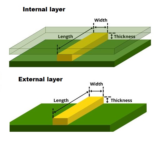
When embarking on a 2oz copper PCB tutorial, understanding design considerations is vital for success. First, consider the trace width and spacing. Thicker copper allows for higher current, but you must still calculate appropriate widths based on expected current loads and temperature rise limits. Tools adhering to IPC-2152, Standard for Determining Current Carrying Capacity in Printed Board Design, can help hobbyists determine safe dimensions for their traces.
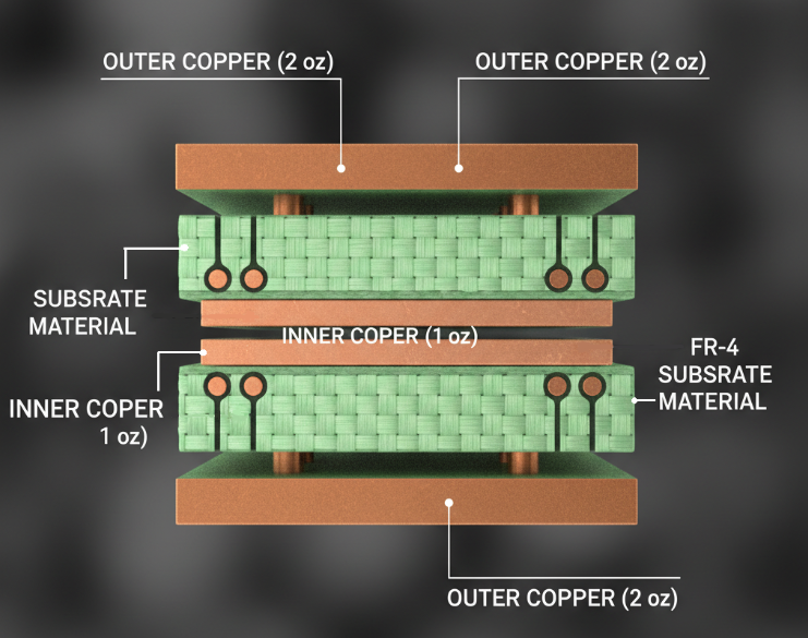
Layer stackup is another factor. In multilayer boards, 2oz copper is often used on outer layers for power distribution, while inner layers might use thinner copper for signal routing. Beginners should plan the stackup early to balance cost and performance. Also, remember that thicker copper can increase the board’s weight and may affect flexibility in designs requiring bending.
Via design needs attention as well. With 2oz copper, vias must be properly sized to handle current and heat without creating weak points. Standards like IPC-A-600K, Acceptability of Printed Boards, provide guidelines on acceptable via structures and plating thickness to ensure reliability.
Finally, consider the thermal expansion differences. Thicker copper can lead to uneven stress during temperature changes, potentially causing warpage. Following design rules from IPC-2221B helps mitigate these risks by ensuring balanced copper distribution across the board.
Practical Tips for Beginner PCB Design with 2oz Copper
Starting with 2oz copper PCB design as a beginner can be straightforward with the right approach. Here are actionable steps to guide you through an easy PCB design process.
- Start with a clear schematic. Before layout, ensure your circuit diagram is complete and accurate. This prevents errors during trace routing and component placement.
- Use design software tools. Many free or low cost tools allow you to set copper thickness and calculate trace widths based on current needs. Look for features that support industry standards like IPC-2152.
- Plan power and ground planes. With 2oz copper, dedicate outer layers to power and ground to maximize current handling and heat dissipation. This also reduces noise in sensitive circuits.
- Keep traces short and direct. Minimize trace length to reduce resistance and potential signal interference, especially in high current areas.
- Verify clearances. Ensure spacing between traces meets minimum requirements to avoid short circuits, as specified in IPC-2221B.
- Test with prototypes. Before final production, create a small batch to test under real conditions. Check for overheating or mechanical issues.
For hobbyists, focusing on simplicity is key. Avoid overcomplicating the design with unnecessary layers or features. Stick to proven layouts and reference designs when possible to build confidence.
Related Reading: Inner Layer Copper Thickness: A Key to Effective PCB Heat Dissipation
Common Challenges and Solutions in 2oz Copper PCB Design
Beginners often face hurdles when working with 2oz copper PCBs. One common issue is underestimating current requirements, leading to narrow traces that overheat. To solve this, always calculate trace widths using guidelines from IPC-2152. Another challenge is uneven copper distribution, which can cause board warpage during thermal cycles. Balance copper across layers by adding dummy fills or adjusting plane areas, as recommended by IPC-2221B.
Manufacturing defects like over etching can also occur with thicker copper, resulting in inaccurate trace widths. Work with fabricators who adhere to IPC-6012E to ensure precise etching and quality control. Additionally, soldering components on thicker copper may require higher temperatures or longer times due to increased heat absorption. Adjust your soldering process accordingly to avoid cold joints.
For hobbyists, troubleshooting these issues early saves time and resources. Always inspect boards visually and test them under load to catch problems before they escalate.
Industry Standards for Reliable 2oz Copper PCB Design
Adhering to recognized standards ensures your 2oz copper PCB meets performance and reliability expectations. The IPC-2221B standard provides comprehensive design guidelines, covering trace width, spacing, and thermal considerations. It is a foundational resource for beginners learning PCB design. Similarly, IPC-2152 offers detailed methods for calculating current carrying capacity, helping you size traces correctly for safety.
For manufacturing quality, IPC-6012E sets performance specifications for rigid boards, including copper thickness tolerances and plating requirements. Visual and structural acceptance criteria are outlined in IPC-A-600K, ensuring your board meets industry benchmarks for defects like voids or cracks.
By integrating these standards into your workflow, you create designs that are not only functional but also manufacturable and durable. Hobbyists can access summaries or guides to these standards through technical libraries or industry associations for a deeper understanding.
Conclusion
Mastering 2oz copper PCB design opens up new possibilities for electronic hobbyists tackling high current and power intensive projects. This beginner PCB design guide has covered the essentials, from understanding the benefits of thicker copper to applying practical tips and adhering to industry standards. By focusing on trace sizing, thermal management, and balanced layouts as outlined in standards like IPC-2221B and IPC-2152, you can create reliable and efficient boards. With practice and attention to detail, your skills in easy PCB design will grow, empowering you to bring innovative ideas to life.
FAQs
Q1: What makes a 2oz copper PCB tutorial important for beginners?
A1: A 2oz copper PCB tutorial helps beginners understand how thicker copper improves current handling and heat dissipation. It guides hobbyists in designing robust boards for power heavy projects. By learning proper trace sizing and layout techniques, you avoid common mistakes like overheating, ensuring safer and more reliable circuits for personal or experimental use.
Q2: How does copper thickness affect my PCB design guide?
A2: Copper thickness, like 2oz, directly impacts current capacity and thermal performance in your PCB design guide. Thicker copper handles higher currents with narrower traces and dissipates heat better. This reduces risks of failure in demanding applications. Standards like IPC-2152 help calculate safe dimensions, ensuring your design meets performance needs.
Q3: What are key challenges in beginner PCB design with 2oz copper?
A3: In beginner PCB design, challenges with 2oz copper include calculating correct trace widths and avoiding warpage from uneven copper distribution. Over etching during manufacturing can also affect precision. Using standards like IPC-2221B for balance and IPC-6012E for quality control helps overcome these issues, making designs more reliable.
Q4: How can I ensure easy PCB design with 2oz copper as a hobbyist?
A4: For easy PCB design with 2oz copper, start with a clear schematic and use software supporting IPC standards. Plan power planes on outer layers, keep traces short, and maintain proper spacing. Test prototypes under load to catch issues early. This structured approach simplifies the process for hobbyists while ensuring functionality.
References
IPC-2221B — Generic Standard on Printed Board Design. IPC, 2012.
IPC-2152 — Standard for Determining Current Carrying Capacity in Printed Board Design. IPC, 2009.
IPC-6012E — Qualification and Performance Specification for Rigid Printed Boards. IPC, 2020.
IPC-A-600K — Acceptability of Printed Boards. IPC, 2020.