Introduction
Polytetrafluoroethylene (PTFE) PCBs represent a cornerstone in high-frequency circuit design, particularly for RF and microwave applications operating above 1 GHz. These boards leverage PTFE’s exceptional electrical properties to minimize signal loss and maintain integrity in demanding environments. Engineers designing radar systems, satellite communications, and 5G infrastructure increasingly rely on PTFE substrates to meet performance benchmarks. This guide delves into PTFE PCB design rules, PTFE PCB impedance control, and PTFE PCB layer stackup strategies, providing structured insights for optimal implementation. By adhering to established engineering principles, designers can achieve reliable signal propagation and reduced electromagnetic interference.
What Are PTFE PCBs and Why Do They Matter for RF and Microwave?
PTFE, commonly known as Teflon, serves as the core dielectric material in these specialized PCBs due to its low dielectric constant and dissipation factor. Typical values include a dielectric constant around 2.1 and a loss tangent of approximately 0.0002 at microwave frequencies, enabling efficient signal transmission with minimal attenuation. In RF and microwave circuits, where wavelengths shorten dramatically, standard FR-4 materials introduce excessive losses and phase shifts. PTFE maintains stable electrical performance across wide frequency ranges and temperatures, making it indispensable for applications like phased array antennas and millimeter-wave modules. Its relevance grows with the expansion of wireless technologies, ensuring compliance with stringent signal integrity requirements.
Beyond electrical advantages, PTFE offers chemical inertness and thermal stability, though it poses unique fabrication challenges. Engineers must balance these traits during design to avoid issues like dimensional instability. Ultimately, PTFE PCBs enable higher operating frequencies and power handling compared to conventional laminates.
Key Material Properties of PTFE for High-Frequency Design
The dielectric constant of PTFE remains nearly constant from DC to beyond 40 GHz, unlike many composites that vary significantly. This stability simplifies modeling and prediction of transmission line behavior in simulation tools. Loss tangent values stay below 0.002 even at elevated frequencies, directly correlating to lower insertion loss in microstrip and stripline configurations. Thermal expansion mismatch between PTFE and copper demands careful selection of foil types, such as low-profile electrodeposited copper, to prevent delamination.
Mechanical properties include a relatively low modulus, leading to potential warpage under thermal stress, which engineers address through symmetric stackups. Moisture absorption is negligible, preserving electrical characteristics in humid environments. These properties collectively position PTFE as the preferred choice for microwave laminates per IPC-6018 qualification standards.
Essential PTFE PCB Design Rules
PTFE PCB design rules prioritize minimizing discontinuities and controlling transmission line geometries to preserve signal fidelity. Trace widths and spacings must account for the low dielectric constant, often resulting in wider traces than FR-4 equivalents for the same impedance. Minimum via sizes and aspect ratios require adjustment due to PTFE’s softness, with plasma cleaning recommended to remove drilling smear without mechanical abrasion.
Routing follows stripline or microstrip topologies, adhering to rules like 3W spacing between traces to suppress crosstalk. Ground plane stitching vias placed at lambda/20 intervals mitigate cavity resonances. Designers apply the 20H rule for isolating RF sections from digital circuitry, where H denotes dielectric height.
Bend radii exceed 2x trace width to avoid radiation losses, and right-angle corners give way to mitered or curved paths. These PTFE PCB design rules ensure compliance with high-frequency performance specs.
Mastering PTFE PCB Impedance Control
PTFE PCB impedance control hinges on precise control of trace geometry, dielectric thickness, and copper roughness. Characteristic impedance formulas for microstrip lines incorporate the low Dk, yielding 50 Ω or 75 Ω with tolerances under ±5%. Field solvers verify designs, factoring in frequency-dependent effects minimal in pure PTFE.
Layer-to-layer variations demand consistent core and prepreg thicknesses, often achieved through hybrid stackups blending PTFE with compatible fillers. VNA or TDR testing post-fabrication confirms targets, as manufacturing tolerances on dielectric height directly impact impedance.
Ground plane proximity controls return path inductance, essential for broadband matching. Engineers iterate stackups to balance impedance uniformity across the board.
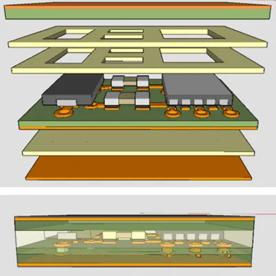
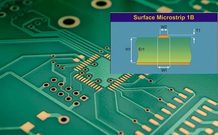
Optimizing PTFE PCB Layer Stackup
PTFE PCB layer stackup design emphasizes symmetry to counteract warpage from CTE differences. Signal layers sandwich between ground planes, with core thicknesses selected for target impedances, such as 0.127 mm for 50-ohm microstrips. Hybrid constructions use ceramic-filled PTFE for outer layers to improve rigidity while preserving inner low-loss cores.
- Top Signal — Microstrip RF — 0.127 mm PTFE core
- Ground — Reference plane — N/A
- Inner Signal — Stripline — 0.254 mm PTFE prepreg
- Bottom Ground — Shielding — N/A
Power and ground plane pairing minimizes loop inductance.
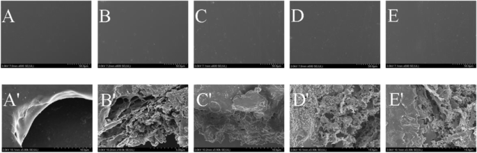
Fabrication and Assembly Considerations
Fabrication of PTFE PCBs requires specialized techniques due to the material’s low modulus and smear propensity. Laser drilling or controlled depth mechanical drilling precedes plasma desmear, avoiding chemical etch-back. Lamination cycles use low ramp rates to prevent voids.
Assembly tolerances tighten for RF connectors, with soldering profiles per J-STD-020 to avoid PTFE degradation. Bake-out precedes reflow to expel absorbed moisture, though minimal.
Post-process inspections verify coplanarity and impedance.
Best Practices and Troubleshooting
Implement full 3D EM simulation early to predict coupling and losses. Prototype with test coupons for TDR validation. Symmetric stackups and uniform copper distribution mitigate warpage.
Common issues like via resonance troubleshoot via backdrilling or filled vias. Document tolerances rigorously for repeatability.
Conclusion
Designing PTFE PCBs for RF and microwave demands meticulous attention to material properties, PTFE PCB design rules, impedance control, and layer stackup. These elements ensure low-loss performance and reliability in high-stakes applications. Engineers equipped with these structured approaches can optimize signal integrity while navigating fabrication nuances. Leveraging standards like IPC-6018 fortifies designs against performance drifts.
FAQs
Q1: What are the primary PTFE PCB design rules for microwave frequencies?
A1: PTFE PCB design rules focus on wide traces for low Dk, mitered bends to reduce reflections, and lambda/20 ground stitching. Maintain 3W trace spacing and symmetric stackups to control warpage. Plasma desmear vias post-drilling. These practices minimize discontinuities and ensure signal fidelity up to mmWave bands.
Q2: How do you achieve precise PTFE PCB impedance control?
A2: PTFE PCB impedance control relies on exact dielectric thicknesses and low-roughness copper. Use microstrip/stripline with adjacent grounds for 50-ohm lines, verified by TDR. Account for minimal Dk variation in models. Hybrid fillers stabilize tolerances below ±5%.
Q3: What is an effective PTFE PCB layer stackup for RF applications?
A3: A robust PTFE PCB layer stackup features signal-ground pairs with 0.127–0.254 mm cores for impedance matching. Symmetry prevents warpage; buried vias shorten stubs. Ground planes shield against EMI. Follow IPC guidelines for layer sequencing.
Q4: Why is PTFE preferred over FR-4 in high-frequency designs?
A4: PTFE’s Dk of 2.1 and Df of 0.0002 yield far lower losses than FR-4’s 4.5 and 0.02. Stability across frequencies suits RF/microwave. Though fabrication-intensive, it excels in phased arrays and 5G.
References
IPC-2221 — Generic Standard on Printed Board Design
J-STD-020 — Moisture/Reflow Sensitivity Classification for Nonhermetic Surface Mount Devices