Introduction
Drilling represents a cornerstone process in PCB manufacturing, enabling the formation of vias and through-holes essential for electrical interconnections in glass-reinforced PCBs. These materials, commonly featuring epoxy resin reinforced with woven glass fibers, provide the structural integrity needed for high-density electronic assemblies. However, the abrasive nature of glass fibers introduces significant hurdles in PCB drilling, including rapid tool wear, heat buildup, and potential defects like burrs or delamination. Electric engineers must grasp these challenges to optimize PCB via formation and ensure reliable performance in demanding applications. This comprehensive guide explores proven drilling techniques, essential tools, and factory best practices tailored for glass-reinforced substrates. By aligning with industry standards, manufacturers can achieve precise hole quality while minimizing production risks.
Understanding Glass-Reinforced PCBs and Drilling Fundamentals
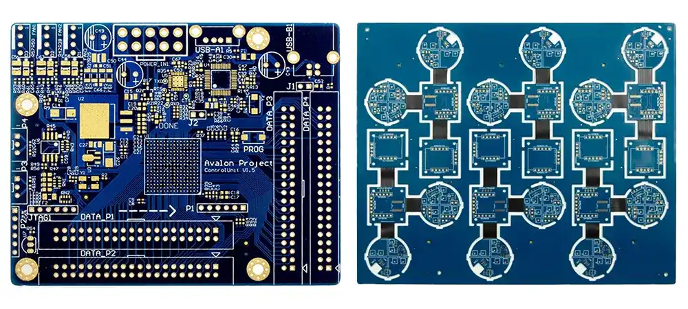
Glass-reinforced PCBs derive their name from the glass fiber cloth embedded within a resin matrix, typically forming laminates that withstand thermal and mechanical stresses. The glass fibers, often E-glass type, create a composite with high tensile strength but exceptional abrasiveness during machining. In PCB manufacturing, drilling creates pathways for plated through-holes (PTH) that connect multiple layers, directly impacting signal integrity and assembly yield. Without proper control, the fibers can cause drill bit deflection or excessive resin smear on hole walls. Factory processes prioritize material-specific parameters to maintain hole wall roughness within acceptable limits. This foundation is critical for advancing to advanced PCB drilling techniques.
The relevance of drilling glass PCBs extends to high-layer-count boards where via density increases complexity. Engineers specify aspect ratios—board thickness to hole diameter—to ensure plating uniformity post-drilling. Glass reinforcement enhances dimensional stability but demands specialized approaches to avoid microcracks from thermal gradients. Production insights reveal that pre-drilling preparation, like panel fixturing, sets the stage for consistent results across batches. Mastering these fundamentals directly influences downstream processes such as desmear and plating.
Key Challenges in Drilling Glass-Reinforced PCBs
The primary obstacle in drilling glass PCBs stems from the silica content in glass fibers, which acts like sandpaper on cutting tools, drastically reducing bit lifespan. Heat generated from friction melts the resin, leading to smear that clogs flutes and degrades hole quality. Common defects include entry and exit burrs, where copper foil lifts or protrudes, and drill wander causing positional inaccuracies. Delamination risks escalate in multilayer stacks if drilling parameters exceed material tolerances. Factory data underscores the need for vigilant process control to mitigate these issues during high-volume PCB via formation.
Rough hole walls from fiber pullout further complicate electroless plating adhesion, potentially causing voids or reliability failures under thermal cycling. Nail heading occurs when inner-layer copper extrudes into the hole, obstructing plating. These challenges amplify in high-aspect-ratio holes common in modern designs. Production teams address them through iterative parameter tuning and inline monitoring. Understanding these pain points equips engineers to select appropriate drilling techniques proactively.
Mechanical Drilling Techniques for Glass-Reinforced PCBs
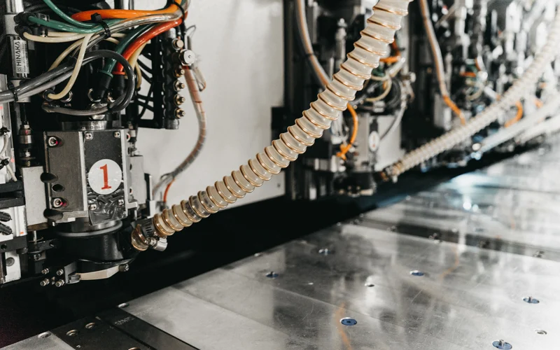
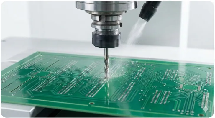
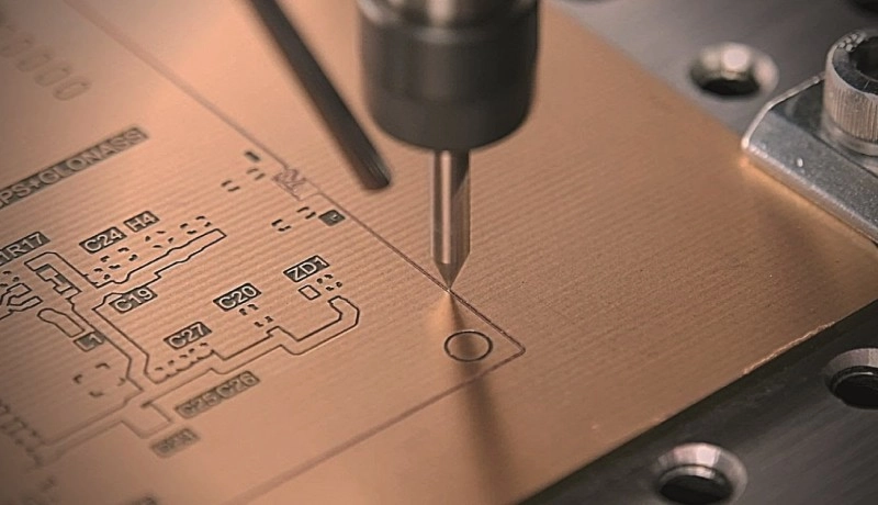
Mechanical drilling remains the workhorse for standard vias in glass-reinforced PCBs, employing high-speed CNC machines with carbide tools. The process involves peck drilling, where the bit retracts periodically to clear chips and reduce heat. Spindle speeds and feed rates must balance penetration efficiency with tool preservation, tailored to board thickness and hole size. Entry and exit materials, such as aluminum foils, prevent burrs by stabilizing the board surface during breakthrough. This technique excels for holes larger than 0.15 mm, supporting efficient PCB manufacturing tips like panel stacking for throughput.
Stack drilling multiple panels simultaneously distributes wear and aligns holes precisely across production runs. Optimal flute geometry, including undercut designs, enhances chip evacuation in abrasive glass matrices. Factories implement thrust force monitoring to detect anomalies early. Post-drill deburring via brushing or plasma ensures clean profiles before desmear. These methods align with guidelines in IPC-DR-572A for achieving consistent hole quality.
Laser Drilling for Precision PCB Via Formation
Laser drilling complements mechanical methods, particularly for microvias under 0.1 mm in glass-reinforced PCBs. UV or CO2 lasers ablate material selectively, minimizing mechanical stress and enabling blind or buried vias. The non-contact nature avoids tool wear, ideal for high-density interconnects (HDI). Process parameters like pulse duration and energy density control taper and heat-affected zones. Factories reserve laser for advanced applications where mechanical limits falter, ensuring taper-free walls for superior plating.
Hybrid approaches combine both techniques for optimized layer access in complex stacks. Laser excels in controlled depth drilling, reducing stub lengths for high-speed signals. Quality verification involves optical profiling for residue-free holes. Production scaling requires cleanroom environments to prevent contamination. This technique revolutionizes PCB via formation in compact electronics.
Essential Tools and Equipment
Carbide drill bits dominate PCB drilling due to their hardness against glass abrasion, outperforming high-speed steel alternatives. Specialized geometries, such as two-flute with polished surfaces, promote smooth entry and efficient chip removal. Spindle systems deliver rotational speeds exceeding 100,000 RPM for fine features. Backup and entry sheets protect panels from splintering. Automated optical inspection (AOI) tools post-drill verify dimensions and defects inline.
Coolants or compressed air manage thermal loads during extended runs. Tool changers enable rapid swaps to maintain hit counts per bit. Fixturing jigs secure panels against vibration. These tools form the backbone of reliable drilling glass PCB operations in factories.
Best Practices for Drilling Glass-Reinforced PCBs
Implement panelization with fiducials for precise registration before drilling. Stack compatible thicknesses to amortize setup time and ensure uniformity. Use mineral oil mist for lubrication in mechanical drilling to dissipate heat without residue. Peck cycles should retract fully to evacuate glass dust effectively. Monitor tool life via hit counters, retiring bits before wear compromises quality. These PCB manufacturing tips stem from factory optimization for yield improvement.
Adhere to IPC-6012F specifications for hole location tolerances and annular ring integrity post-plating. Conduct cross-section analysis on pilot panels to validate wall roughness. Employ automated deburring to standardize surfaces. Sequence drill larger holes first to minimize stress on finer ones. Regular machine calibration prevents drift over shifts.
Inline metrology confirms drill-to-drill alignment within microns. Desmear processes like plasma or permanganate etch remove resin smear uniformly. Quality gates per IPC-A-600M reject boards with excessive breakout or roughness. Document parameters for traceability across lots. These practices ensure robust PCB via formation.
Troubleshooting Common Drilling Issues
Burrs at entry or exit signal inadequate backing materials; switch to phenolic sheets for better support. Excessive smear indicates high feed rates; reduce incrementally while monitoring thrust. Drill wander in small diameters points to dull bits or misalignment; sharpen or recalibrate. Delamination from heat requires coolant enhancement or speed reduction. Nail heading demands adjusted inner-layer etchback.
- Burrs — Cause: Poor entry/exit; Remedy: Upgrade foils, optimize peck
- Smear — Cause: Friction heat; Remedy: Lubricate, lower feed
- Wander — Cause: Tool wear; Remedy: Monitor hits, inspect bits
- Rough walls — Cause: Fiber abrasion; Remedy: Peck drill, polish flutes
Cross-section sampling identifies root causes systematically. Adjust for material variations like fiber weave direction. These factory-driven solutions restore process control swiftly.
Conclusion
Drilling glass-reinforced PCBs demands a blend of precise techniques, durable tools, and rigorous best practices to overcome material challenges. From mechanical peck drilling to laser precision, each method contributes to flawless PCB via formation. Factory insights emphasize parameter optimization, standard compliance, and proactive troubleshooting for high yields. Electric engineers benefit from these strategies in designing manufacturable boards. Prioritizing hole quality upfront enhances overall PCB reliability and performance.
FAQs
Q1: What are the main challenges in PCB drilling for glass-reinforced materials?
A1: The abrasive glass fibers accelerate tool wear and generate heat, leading to defects like burrs, smear, and delamination. Factories mitigate this through peck drilling and lubrication. Proper entry materials prevent breakout issues. Adhering to drilling techniques ensures clean vias for plating. These factors directly affect PCB manufacturing tips for consistent quality.
Q2: How do mechanical and laser drilling differ in PCB via formation?
A2: Mechanical drilling suits larger through-holes with carbide bits, offering high throughput via stacking. Laser excels for microvias, providing non-contact precision without wear. Each has optimized parameters for glass substrates. Factories select based on hole size and board type. Combining them optimizes HDI designs.
Q3: Why is tool selection critical for drilling glass PCBs?
A3: Stack panels, use entry/exit foils, and monitor tool life closely. Peck cycles clear chips effectively in glass matrices. Inline inspection catches defects early. Calibrate machines regularly for accuracy. These practices align with standards for reliable hole quality.
Q4: Why is extended temperature range AI PCB critical for industrial edge computing?
A4: Carbide bits resist abrasion better than alternatives, extending life in fiber-rich materials. Geometry affects chip evacuation and heat control. Factories track hit counts to prevent failures. Proper selection minimizes downtime and defects in production.
References
IPC-DR-572A — Drilling Guidelines for Printed Boards. IPC, 2007
IPC-6012F — Qualification and Performance Specification for Rigid Printed Boards. IPC, 2023
IPC-A-600M — Acceptability of Printed Boards. IPC, 2025