Introduction
In the design of 4-layer printed circuit boards, managing heat dissipation is a critical challenge, especially for high power components. Excessive heat can degrade performance, reduce component lifespan, and cause system failures. Thermal vias offer a proven solution by providing low resistance paths for heat transfer from hot spots to cooler layers or heat sinks. For electrical engineers, understanding 4-layer PCB thermal via placement is essential to ensure efficient cooling and maintain reliability. This article explores the principles of 4-layer PCB heat dissipation, key cooling techniques, and best practices for optimizing thermal resistance in designs with high power components. By applying these strategies, engineers can enhance the thermal performance of their boards and meet stringent operational demands.
What Are Thermal Vias and Why Do They Matter in 4-Layer PCBs
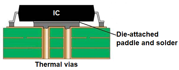
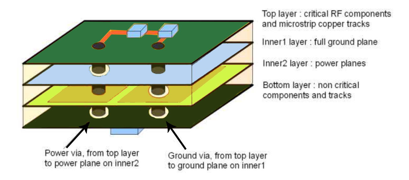
Thermal vias are small, plated through holes in a printed circuit board that facilitate heat transfer between layers. In a four layer PCB, they typically connect the top and bottom copper layers to inner ground or power planes, which act as heat spreaders. Their primary role is to reduce thermal resistance by creating direct paths for heat to escape from high power components to areas with better cooling potential. Effective 4-layer PCB heat dissipation is vital because modern electronics often involve densely packed components generating significant heat. Without proper management, localized hot spots can lead to thermal stress, impacting reliability. For engineers, mastering 4-layer PCB cooling techniques ensures designs can handle increased power densities while maintaining stability and performance under load.
Technical Principles of Thermal Vias in 4-Layer PCBs
Thermal vias work by leveraging the high thermal conductivity of copper to move heat away from critical areas. In a 4-layer PCB, the stackup usually consists of two signal layers on the top and bottom, with internal ground and power planes. When placed near high power components, thermal vias create a conduit for heat to flow from the component's thermal pad to the inner planes or an external heat sink. The effectiveness of 4-layer PCB thermal resistance reduction depends on several factors, including via size, spacing, and the number of vias in an array. Smaller vias allow denser placement but may offer less heat transfer capacity. Larger vias conduct more heat but occupy valuable board space. Additionally, filling vias with conductive materials can enhance performance, though this must comply with manufacturing standards like IPC-6012E.
The placement of vias directly under or around heat generating components maximizes their impact. Heat flows through the path of least resistance, so connecting vias to large copper planes or external cooling mechanisms is critical. Engineers must also consider the thermal conductivity of the PCB material itself, as standard FR-4 has limitations compared to high thermal conductivity laminates. Balancing these elements ensures optimal 4-layer PCB heat dissipation without compromising signal integrity or layout constraints.
Best Practices for Thermal Via Placement in 4-Layer PCBs
Optimizing 4-layer PCB cooling techniques requires careful planning during the design phase. Below are actionable strategies for effective thermal via placement tailored to high power components.
Strategic Location for Maximum Heat Transfer
Place thermal vias as close as possible to the heat source, ideally directly beneath the thermal pad of high power components. This minimizes the distance heat must travel, reducing thermal resistance. For components with exposed pads, ensure vias connect directly to the pad and link to a large copper area on the opposite side or inner layers. Distribute vias evenly in a grid pattern to avoid creating localized heat concentrations.
Determining Via Size and Count
The size and number of thermal vias impact their effectiveness in 4-layer PCB heat dissipation. Smaller vias, often around 0.3 to 0.5 mm in diameter, allow for higher density but transfer less heat per via. Larger vias can handle more heat but may interfere with routing. A common practice is to use an array of smaller vias to balance heat transfer and space constraints. The total cross-sectional area of copper in the vias should be maximized while adhering to manufacturing limits outlined in standards like IPC-A-600K.
Connecting to Copper Planes
Link thermal vias to substantial copper areas, such as ground or power planes in the 4-layer PCB stackup. These planes act as heat spreaders, distributing thermal energy across a wider area for dissipation. Ensure minimal interruptions in the copper plane around the vias to maintain a continuous path for heat flow. Avoid placing signal traces or cuts in the plane near thermal via arrays, as this can disrupt heat transfer.
Suggested Reading: Power and Ground Plane Design in 4 Layer PCBs
Consideration of Via Fill and Plating
Unfilled vias can trap air, reducing their thermal conductivity. For high performance designs, consider specifying via fill with conductive epoxy or copper plating to enhance heat transfer. This process, while increasing manufacturing complexity, can significantly lower 4-layer PCB thermal resistance. Ensure the chosen method aligns with guidelines in IPC-6012E to maintain reliability during fabrication.
Balancing with Electrical Design Constraints
While focusing on 4-layer PCB cooling techniques, engineers must avoid compromising electrical performance. Thermal vias connected to ground planes can introduce parasitic capacitance or affect signal integrity if placed near high speed traces. Isolate thermal via arrays from sensitive signals or use dedicated thermal pads disconnected from electrical nets when necessary. This ensures thermal management does not interfere with the primary function of the circuit.
Advanced Strategies for High Power Components in 4-Layer PCBs
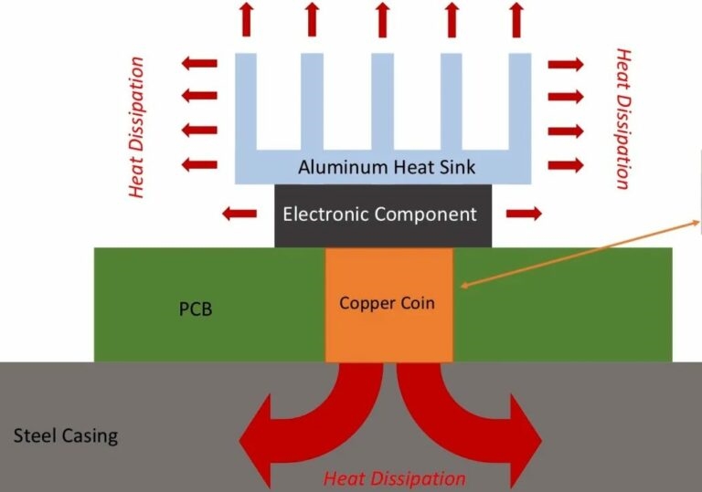
High power components, such as voltage regulators, power amplifiers, or microprocessors, generate significant heat, demanding advanced 4-layer PCB heat dissipation approaches. Beyond basic thermal via placement, consider integrating larger heat sinks or thermal pads on the board surface. Position thermal vias to connect directly to these cooling elements, creating a seamless path for heat to exit the system. For extremely high power applications, engineers can explore via stitching, where multiple layers of vias are aligned to form a robust thermal conduit through the board.
Another technique involves optimizing the PCB material itself. While standard FR-4 is common in 4-layer designs, its thermal conductivity is relatively low. Materials with enhanced thermal properties, often specified under standards like IPC-4101, can improve overall heat management when paired with thermal vias. Additionally, ensure proper airflow or forced cooling over the board in the final enclosure to complement the via based heat dissipation strategy.
Challenges and Troubleshooting in Thermal Via Implementation
Implementing thermal vias in 4-layer PCBs is not without challenges. One common issue is manufacturing variability, where vias may not be plated uniformly, reducing their effectiveness. Adhering to quality standards like IPC-A-600K during fabrication can mitigate this risk by ensuring consistent plating thickness. Another challenge is thermal via overcrowding, which can weaken the board structure or complicate routing. Engineers should simulate thermal performance during the design phase using appropriate tools to predict hot spots and adjust via placement accordingly.
If heat dissipation remains inadequate despite via placement, consider revisiting the overall layout. Spreading out high power components or increasing copper thickness on outer layers can provide additional relief. Always verify the thermal design against real world conditions, as theoretical models may not account for enclosure effects or ambient temperature variations.
Conclusion
Effective thermal management in 4-layer PCBs is crucial for maintaining the reliability and performance of modern electronic designs, particularly those with high power components. Thermal vias play a pivotal role in reducing 4-layer PCB thermal resistance by providing efficient heat dissipation paths. By strategically placing vias near heat sources, connecting them to large copper planes, and considering advanced techniques like via fill, engineers can significantly enhance 4-layer PCB cooling techniques. Balancing thermal and electrical design constraints ensures optimal performance without compromising functionality. Adhering to industry standards like IPC-6012E and IPC-A-600K during design and manufacturing further guarantees success. With these practices, electrical engineers can tackle the challenges of heat management in compact, high density 4-layer PCB layouts.
FAQs
Q1: How do thermal vias improve 4-layer PCB heat dissipation?
A1: Thermal vias improve 4-layer PCB heat dissipation by creating low resistance paths for heat to travel from high power components to cooler areas like ground planes or heat sinks. Positioned near heat sources, they transfer thermal energy efficiently through copper plating. Their effectiveness depends on proper placement, size, and connection to large copper areas, ensuring reduced thermal stress and enhanced reliability in compact designs.
Q2: What factors affect 4-layer PCB thermal resistance with vias?
A2: Several factors influence 4-layer PCB thermal resistance when using vias, including via size, count, and placement near heat sources. Connection to substantial copper planes enhances heat spreading, while via fill with conductive materials can lower resistance. PCB material thermal conductivity and manufacturing quality, as per standards like IPC-6012E, also play significant roles in determining overall thermal performance.
Q3: What are key 4-layer PCB cooling techniques for high power components?
A3: Key 4-layer PCB cooling techniques for high power components include placing thermal vias directly under thermal pads, connecting them to inner copper planes, and using heat sinks for additional dissipation. Optimizing via arrays for density and fill, ensuring airflow in enclosures, and selecting materials with better thermal properties are also vital. These methods collectively prevent overheating and maintain component longevity.
Q4: How many thermal vias are needed for effective 4-layer PCB cooling?
A4: The number of thermal vias needed for effective 4-layer PCB cooling depends on the heat generated by components and the board's thermal design. A grid pattern under high power components, balancing via size and spacing, often works best. Engineers should simulate heat distribution to determine the optimal count while adhering to manufacturing constraints outlined in standards like IPC-A-600K.
References
IPC-6012E — Qualification and Performance Specification for Rigid Printed Boards. IPC, 2020.
IPC-A-600K — Acceptability of Printed Boards. IPC, 2020.
IPC-4101E — Specification for Base Materials for Rigid and Multilayer Printed Boards. IPC, 2021.