Introduction
In modern PCB design, effective via placement plays a critical role in achieving reliable signal routing, particularly for high-speed applications. Through-hole vias serve as essential interconnects between layers, but their positioning directly impacts signal integrity, impedance control, and electromagnetic interference. Poor via placement can lead to increased crosstalk, reflections, and return path disruptions, compromising overall board performance. Engineers must consider stackup configuration, trace lengths, and plane interactions when strategizing via locations. This article explores proven strategies for through-hole via placement to optimize PCB routing and signal routing efficiency. By focusing on structured approaches, designers can enhance high-speed routing outcomes without unnecessary complexity.
Understanding Through-Hole Vias and Their Role in Signal Routing
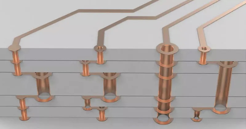
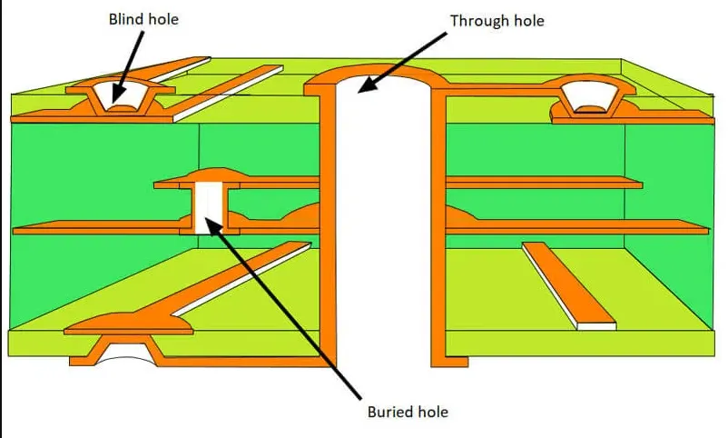
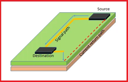
Through-hole vias are plated holes that extend fully through the PCB stackup, providing vertical interconnections for signals, power, and ground. Unlike blind or buried vias, they connect all layers, making them suitable for multi-layer boards where comprehensive layer access is needed. In signal routing, these vias introduce discontinuities that affect characteristic impedance, especially in high-speed environments where frequencies exceed hundreds of MHz. Proper via placement ensures minimal stub length and maintains continuous reference planes for return currents. Why does this matter? Suboptimal placement disrupts ground return paths, leading to signal degradation and higher bit error rates in digital systems.
The relevance intensifies in dense boards with mixed signal types, where via placement influences crosstalk between adjacent traces. Standards like IPC-2221 outline general guidelines for via integrity and spacing to support manufacturability and performance. Engineers prioritize via placement during initial layout planning to avoid routing bottlenecks later. This foundational understanding allows for proactive design decisions that align with high-speed routing demands.
Technical Principles Governing Via Placement
Via placement in PCB routing hinges on electromagnetic principles, particularly the need for low-inductance paths and controlled impedance. Each through-hole via creates a parasitic inductance proportional to its length and diameter, which can cause voltage drops and ringing in high-speed signals. To mitigate this, vias must align closely with signal traces to preserve return path integrity under adjacent ground planes. Ground vias, placed strategically near signal vias, facilitate stitching between planes, reducing loop inductance. Signal routing benefits from symmetric via arrangements in differential pairs, ensuring balanced propagation delays.
Return path continuity represents a core mechanism. High-frequency currents follow the path of least impedance, preferring solid planes over split regions. When a signal changes layers via a through-hole via, the return current must transition seamlessly through nearby ground vias. Disruptions, such as plane splits without stitching, force longer detours, amplifying EMI. Via placement density affects thermal management too, as clustered vias can create hotspots, though this ties back to current distribution uniformity.
Impedance matching further dictates strategies. Through-hole vias alter local impedance unless compensated by anti-pad sizing and barrel plating thickness per design standards. In high-speed routing, engineers model via transitions using field solvers to predict insertion loss. Placement near component pins minimizes escape routing lengths, reducing overall discontinuities.
Best Practices for Through-Hole Via Placement in PCB Routing
Start with floorplanning to position components optimally, allowing short, direct via placements for critical signals. In high-speed routing, dedicate inner layers as solid ground planes beneath signal layers to provide stable references. Place through-hole vias perpendicular to planes to avoid oblique angles that increase inductance. For via stitching, array ground vias along trace edges or plane boundaries at consistent pitches, ensuring multiple low-impedance return paths. This technique, common in RF sections, ties split planes effectively without capacitors.
When implementing ground vias, position them adjacent to signal vias during layer transitions. Ideally, sandwich a ground via between paired signal vias in differential routing to maintain symmetry and shield crosstalk. Avoid placing vias in high-current paths without sufficient density to distribute heat evenly. IPC-6012 provides qualification criteria for via reliability under thermal stress, emphasizing plating uniformity.
Optimize via placement by minimizing layer hops for high-speed nets; reserve through-hole vias for power or low-speed signals where stubs are tolerable. Backdrilling, if feasible, shortens stubs on unused layers, preserving signal routing quality. In dense areas, use grid patterns for stitching vias to prevent isolated plane sections. Regularly review DRC violations for spacing, ensuring via-to-via clearances support fabrication tolerances.
- Signal Through-Hole Via — Place near trace entry/exit points and align with a continuous reference plane to reduce stub effects and maintain impedance.
- Ground Via — Position 1–2× trace width from the signal via to provide a low-inductance return path during layer transitions.
- Stitching Via Array — Deploy along plane edges or splits with uniform spacing to ensure plane continuity and minimize EMI.
Challenges in Via Placement and Troubleshooting Insights
Designers often encounter plane splits interrupting return paths, especially in multi-layer boards with partitioned power/ground. Troubleshooting involves identifying via-induced resonances via time-domain reflectometry simulations. Relocate ground vias to bridge splits, or add stitching arrays if redesign allows. Another issue arises from via clustering near connectors, causing impedance mismatches; disperse them while preserving short routes.
High-speed routing exacerbates via stub effects in thick boards, where aspect ratios challenge plating quality. Select via diameters balancing drill feasibility and inductance, guided by stackup calculations. Fabricators flag excessive via density as yield risks, so balance performance with manufacturability. Case in point: a 10-layer board redesign shifted stitching vias closer to DDR traces, slashing eye diagram jitter by ensuring robust ground returns.
Thermal vias disguised as ground vias aid component cooling but require placement away from sensitive analog sections to avoid noise coupling. Verify post-layout stackup integrity to confirm no orphaned vias disrupt fields.
Conclusion
Mastering through-hole via placement elevates PCB routing from adequate to optimal, particularly for signal routing in high-speed contexts. Key strategies like via stitching, strategic ground vias, and impedance-aware positioning ensure signal integrity and EMI compliance. Logical planning from floorplanning through verification minimizes risks. Engineers applying these principles achieve reliable boards aligned with industry benchmarks. Future designs will leverage denser stackups, demanding even finer via placement control. Prioritize these tactics for superior high-speed routing performance.
FAQs
Q1: What is via stitching and how does it improve signal routing?
A1: Via stitching involves placing multiple ground vias along plane edges or near high-speed traces to connect reference planes. This creates low-impedance return paths, reducing inductance and EMI in PCB routing. Proper spacing ensures uniform current distribution, vital for high-speed routing. Follow consistent pitches to avoid hotspots.
Q2: Why place ground vias near through-hole signal vias?
A2: Ground vias adjacent to signal vias provide immediate return paths during layer changes, preserving signal integrity. This setup minimizes loop areas that induce crosstalk in high-speed environments. In differential pairs, it maintains balance. Essential for optimal via placement strategies.
Q3: How does via placement affect high-speed PCB routing?
A3: Strategic via placement controls impedance discontinuities and supports continuous ground planes under traces. Poor placement leads to reflections and signal degradation. Use arrays for stitching in dense areas. Aligns with standards for reliable performance.
Q4: What common mistakes occur in through-hole via placement?
A4: Clustering vias without spacing causes fabrication issues and uneven plating. Ignoring return paths across plane splits amplifies noise. Overlooking stub lengths in thick boards degrades high-speed signals. Plan early to integrate ground vias effectively.
References
IPC-2221B — Generic Standard on Printed Board Design. IPC, 2012
IPC-6012E — Qualification and Performance Specification for Rigid Printed Boards. IPC, 2017
IPC-A-600K — Acceptability of Printed Boards. IPC, 2020