Introduction
Through-hole vias, also known as plated through-holes, serve as critical interconnects in multilayer printed circuit boards, carrying signals and power between layers. These structures consist of a drilled hole electroplated with copper to form a conductive barrel connecting pads on opposite sides of the board. In high-reliability applications such as aerospace, automotive, and telecommunications, via reliability directly impacts overall PCB performance and longevity. Failures in these vias can lead to open circuits, intermittent connections, or complete board malfunction, often manifesting after prolonged use under thermal or mechanical stress. Understanding common failure modes through PCB failure analysis helps engineers design and manufacture boards that withstand real-world conditions. This article explores key failure mechanisms like via cracking, via electromigration, and thermal stress effects, while outlining prevention strategies aligned with industry standards.
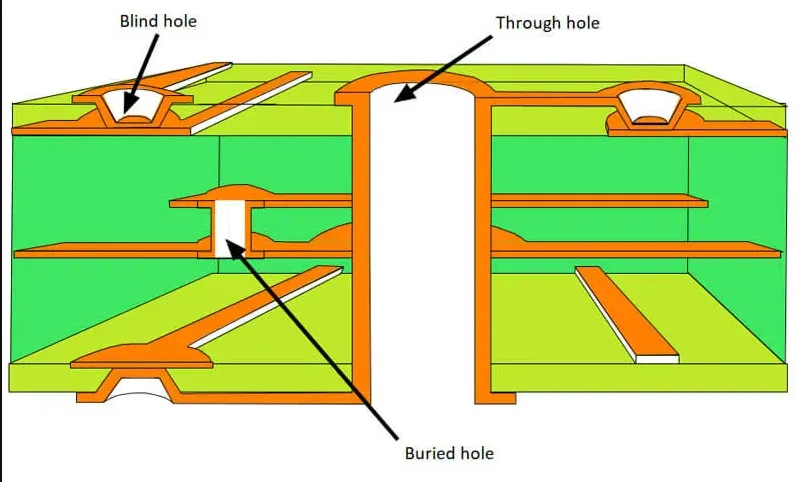
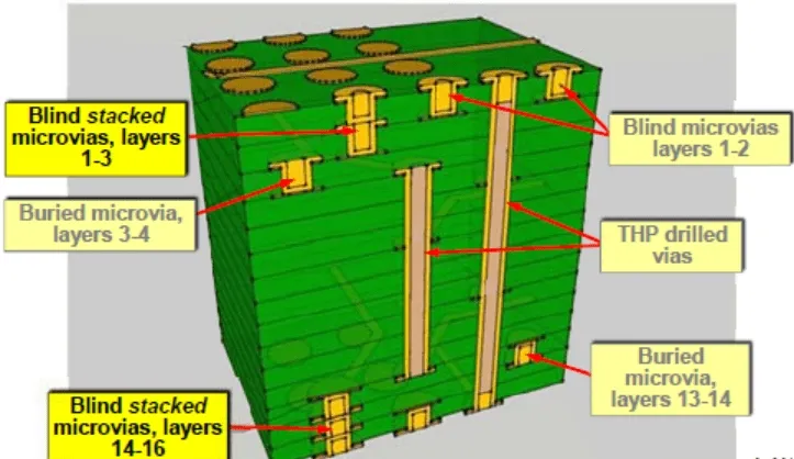
Understanding Through-Hole Vias and Their Role in PCB Reliability
Through-hole vias provide robust mechanical strength compared to surface-mount alternatives, making them suitable for components requiring high pin counts or power handling. They involve drilling, desmearing, electroless copper seeding, and electroplating to build up the barrel wall thickness. Reliability concerns arise primarily from the interface between the copper plating and the dielectric material, where differential expansion during temperature changes induces stress. In factory settings, via reliability determines yield rates and field performance, especially in Class 3 assemblies per IPC standards. Poor via integrity can cascade into system-level failures, underscoring the need for rigorous process controls during manufacturing. Engineers must prioritize via design and fabrication parameters to ensure long-term stability.
Via reliability becomes paramount in environments with frequent thermal cycling, high current loads, or mechanical vibrations. Factory-driven insights reveal that most via issues stem from process variations rather than inherent design flaws. By adhering to qualification tests outlined in IPC-6012, manufacturers can verify via performance under simulated operating conditions. This proactive approach minimizes risks associated with PCB failure analysis post-production.
Common Failure Modes in Through-Hole Vias
Via Cracking
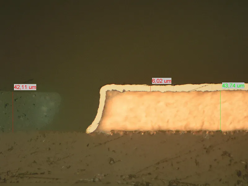
Via cracking represents one of the most prevalent failure modes identified in PCB failure analysis, often appearing as circumferential fractures in the copper barrel. These cracks initiate at the copper-dielectric interface due to repeated mechanical fatigue. During thermal excursions, the laminate expands more in the z-axis than the copper plating, generating tensile stress that propagates cracks over cycles. Factory inspections frequently detect early signs through cross-sectioning or electrical testing. In severe cases, cracks lead to intermittent conductivity, compromising signal integrity. Prevention starts with optimizing plating processes to achieve uniform adhesion and thickness.
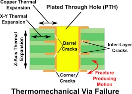
Manufacturing data shows via cracking accelerates in boards with high aspect ratios or inadequate desmear, trapping residues that weaken the barrel. Engineers conducting PCB failure analysis use dye-and-peel tests to map crack locations and severity. Aligning fabrication with IPC-A-600 acceptability criteria helps classify and reject suspect vias early.
Via Electromigration
Via electromigration occurs when high current densities cause copper atoms to migrate, forming voids and hillocks within the plating. This mass transport phenomenon intensifies at elevated temperatures and under direct current bias, depleting material from the cathode end of the via. Over time, voids enlarge, increasing resistance and risking open failures. PCB failure analysis via resistance monitoring or thermal imaging reveals hotspots indicative of electromigration. Factory processes must limit current per via cross-section to avoid exceeding critical thresholds. Material purity and grain structure in the plating play key roles in mitigating this mode.
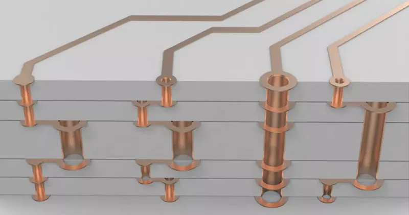
In multilayer boards, stacked vias amplify electromigration risks due to cumulative current paths. Engineers mitigate this by distributing loads across multiple vias or using wider barrels. Long-term reliability testing simulates operating currents to predict electromigration lifetimes.
Thermal Stress Failures
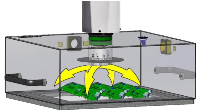
Thermal stress induces failures through coefficient of thermal expansion mismatches between copper and laminate materials. During soldering or operational heating, compressive and tensile forces strain the via barrel, leading to delamination or cracking. PCB warpage exacerbates this, pulling vias away from pads. Factory-driven thermal profiling ensures profiles stay within material limits. PCB failure analysis often employs thermal cycling chambers to replicate field conditions. Adopting low-CTE laminates reduces stress accumulation.
Additional modes include plating voids from poor activation and blow holes from moisture entrapment. These defects create weak points prone to propagation under stress.
Mechanisms Behind Via Failures
The primary mechanism for via cracking involves cyclic fatigue from z-axis expansion differentials. Copper plating, with its low CTE, resists expansion while the resin swells, shearing the interface. Microvoids form at plating boundaries, coalescing into cracks after thousands of cycles. Electromigration follows Black's equation, where lifetime inversely scales with current density exponent and temperature activation energy. Thermal stress compounds both by elevating local temperatures and strains.
Factory processes like sequential lamination introduce residual stresses that precondition vias for failure. Drilling-induced microcracks serve as crack initiation sites if not properly desmeared. Comprehensive understanding guides process refinements for enhanced via reliability.
Prevention Strategies and Best Practices
Preventing via failures begins with design rules favoring lower aspect ratios and generous annular rings. Fabricators recommend via diameters scaled to board thickness for optimal plating distribution. Employing pulse plating enhances uniformity and reduces internal stresses in the copper barrel. Pre-baking boards removes absorbed moisture, averting voids during lamination or reflow.
Process controls per IPC standards ensure minimum plating integrity. Thermal shock testing per IPC-TM-650 validates resistance to rapid temperature changes. For electromigration, current derating and thermal vias aid heat dissipation.
In manufacturing, automated optical inspection flags potential defects early. Selecting high-Tg laminates minimizes CTE mismatch effects. Post-plating anneals relieve hydrogen embrittlement in copper.
PCB Failure Analysis Techniques for Vias
Effective PCB failure analysis employs non-destructive methods like X-ray to detect voids or cracks without sectioning. Electrical testing under bias accelerates electromigration for failure prediction. Cross-section microscopy provides definitive evidence of barrel integrity. Dye penetrant highlights fissures invisible to the eye.
Factory labs integrate these with scanning electron microscopy for elemental analysis. Trending data from multiple boards identifies systemic process drifts. This insight refines via reliability across production runs.
Conclusion
Through-hole via reliability hinges on addressing cracking, electromigration, and thermal stress through informed design and manufacturing. Factory-aligned practices, grounded in IPC standards, deliver boards resilient to demanding environments. By integrating rigorous testing and process controls, engineers avert costly field failures. Prioritizing PCB failure analysis fosters continuous improvement in via performance. Ultimately, robust vias ensure system reliability, supporting innovation in electronics.
FAQs
Q1: What causes via cracking in PCBs, and how does it relate to thermal stress?
A1: Via cracking primarily results from CTE mismatch between copper plating and laminate during thermal cycling, generating fatigue stresses. Thermal stress accelerates crack propagation by inducing repeated expansion-contraction cycles. PCB failure analysis via cross-sectioning confirms circumferential fractures at the interface. Manufacturers prevent this by using low-CTE materials and adhering to IPC standards for plating quality. Regular thermal profiling in production minimizes risks.
Q2: How can engineers improve via reliability against electromigration?
A2: Via electromigration arises from high current densities causing atomic migration and voids. Improve reliability by sizing vias for lower current densities and distributing loads across parallels. Enhanced plating processes yield finer grains resistant to migration. Accelerated life testing predicts performance under bias. Factory monitoring of current paths ensures compliance with design margins.
Q3: What role do IPC standards play in PTH via prevention strategies?
A3: IPC standards like IPC-6012 outline qualification for rigid boards, specifying via performance criteria. They guide plating thickness, hole quality, and testing protocols for reliability. IPC-A-600 provides visual acceptability for manufacturing inspections. Compliance reduces via cracking and electromigration incidents. Engineers reference these for consistent, factory-proven outcomes.
Q4: How does PCB warpage contribute to via failures under thermal stress?
A4: PCB warpage induces mechanical bending that stresses via barrels, compounding thermal expansion effects. Convex or concave bowing pulls plating from walls, initiating cracks. Mitigation involves symmetric stackups and controlled cooling rates post-lamination. Thermal stress testing reveals warpage impacts on via reliability. Balanced copper distribution prevents uneven strains.
References
IPC-6012E — Qualification and Performance Specification for Rigid Printed Boards. IPC, 2017
IPC-A-600K — Acceptability of Printed Boards. IPC, 2020
IPC-TM-650 2.6.8 — Thermal Shock. IPC, 2018