Introduction
Creating an 8-layer printed circuit board as a DIY project is a rewarding yet complex endeavor for electronic hobbyists. These multilayer boards enable compact designs with high functionality, often used in advanced projects like embedded systems or high-speed digital circuits. However, the increased layer count introduces unique challenges, from short circuits to open circuits, that can derail a project. This comprehensive PCB troubleshooting guide addresses common issues in DIY 8-layer PCBs, offering practical solutions for fixing short circuits, identifying open circuits, testing PCB continuity, and applying rework techniques. Whether you are debugging a prototype or refining a design, understanding these problems and their solutions will elevate your skills and ensure reliable outcomes in your electronic projects.
What Are 8-Layer PCBs and Why Do They Matter
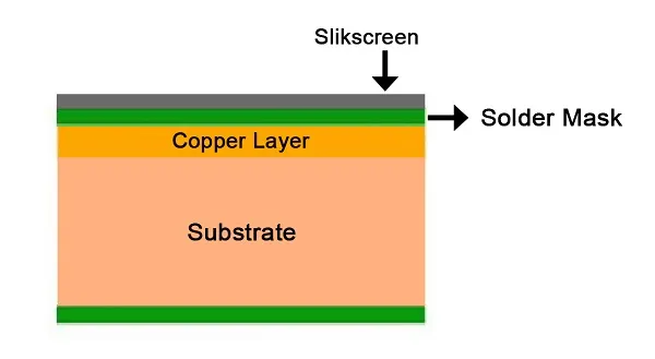
An 8 layer PCB consists of eight conductive copper layers separated by insulating materials, typically used for complex circuits requiring dense routing and noise isolation. Electronic hobbyists often turn to these boards for projects involving microcontrollers, RF applications, or high-speed data transfer, where single or double-layer boards fall short. The multiple layers allow for dedicated power and ground planes, reducing electromagnetic interference and improving signal integrity. However, the complexity of 8-layer designs amplifies the risk of manufacturing defects and assembly errors. Issues like short circuits between layers or broken traces can be harder to detect and fix compared to simpler boards. Mastering troubleshooting for these PCBs is essential to ensure functionality and avoid costly redesigns or wasted materials in DIY projects.
Technical Causes of Common Issues in 8-Layer PCBs
Short Circuits in Multilayer Designs
Short circuits occur when unintended electrical connections form between two conductive paths, often due to manufacturing flaws or design oversights. In 8-layer PCBs, shorts can happen between adjacent layers if the insulating dielectric material is too thin or damaged during drilling. Misaligned vias or burrs from poor drilling can also bridge layers. Additionally, excess solder during assembly might create unintended connections, especially in densely packed areas. These faults can lead to erratic behavior or complete failure of the circuit, making fixing short circuits a priority for hobbyists.
Open Circuits and Trace Failures
An open circuit results from a break in the conductive path, preventing current flow to critical components. In 8-layer PCBs, opens can stem from cracked traces due to mechanical stress, poor etching during fabrication, or incomplete via plating. Identifying open circuits is challenging in multilayer boards because the fault may lie in an internal layer, hidden from visual inspection. Such issues often manifest as non-functional sections of the circuit, requiring systematic testing to pinpoint the break.
Continuity Problems Across Layers
Continuity issues arise when connections between layers, typically through vias, fail to conduct properly. This can happen due to incomplete via filling, delamination of layers under thermal stress, or corrosion over time. In DIY 8-layer PCBs, hobbyists might encounter these problems if the fabrication process lacks precision or if thermal profiles during soldering are not controlled. Poor continuity disrupts signal paths, leading to intermittent failures or degraded performance in high-speed applications.
Suggested Reading: Signal Integrity for Hobbyists: Simple Tips for Better 8 Layer PCB Designs
Practical Solutions for Troubleshooting 8-Layer PCBs
Step-by-Step PCB Troubleshooting Guide
Troubleshooting an 8-layer PCB requires a methodical approach to isolate and resolve issues. Start with a visual inspection under good lighting or magnification to spot obvious defects like solder bridges, cracked traces, or misaligned components. Use a multimeter for testing PCB continuity across traces and vias, ensuring each path conducts as expected. For deeper issues, consider thermal imaging to detect hot spots indicative of shorts, though this may require specialized tools beyond a typical hobbyist setup. Document each test to avoid repeating steps and to track potential failure points.
Fixing Short Circuits in Dense Layouts
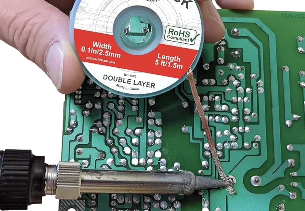
To address short circuits, begin by isolating the affected area through continuity testing with a multimeter set to the lowest resistance range. Check between adjacent pins, traces, or planes to locate unintended connections. If a short is found, carefully remove excess solder using a desoldering wick or pump, ensuring not to damage nearby components. For interlayer shorts, which are harder to access, inspect via barrels for defects using magnification. If the short persists, it may indicate a fabrication flaw, requiring advanced rework techniques or a board redesign.
Identifying Open Circuits in Hidden Layers
When suspecting an open circuit, use a multimeter in continuity mode to test between endpoints of a suspected trace or via. Start at component pads and work inward, checking each segment. If the break is in an internal layer, external testing may not suffice, and hobbyists might need to rely on design schematics to infer the fault location. In some cases, applying a small voltage and observing current flow with a sensitive meter can help confirm the break. Repairing internal opens often requires professional equipment, but surface breaks can be bridged with fine wire and solder as a temporary fix.
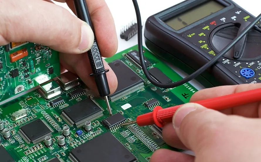
Testing PCB Continuity for Reliable Connections
Testing PCB continuity is fundamental to ensuring all connections function as intended. Set a multimeter to continuity mode and probe between points that should be connected, such as via ends or trace endpoints. A beep or low resistance reading confirms a good connection. Test systematically across all critical paths, especially power and ground planes, to rule out partial failures. For 8-layer boards, focus on vias connecting internal layers, as these are common failure points. Consistent testing prevents overlooking subtle issues that could affect performance.
Rework Techniques for DIY Repairs
Reworking a PCB involves repairing or replacing components and traces without damaging the board. For surface issues, use a soldering iron with a fine tip to remove and replace faulty components, applying flux to ensure clean joints. When dealing with multilayer boards, avoid excessive heat to prevent delamination of internal layers, adhering to guidelines like those in IPC-7711/7721 for rework and repair. For broken traces, carefully scrape away solder mask to expose copper, then solder a small jumper wire to bridge the gap. Practice on scrap boards to build confidence before attempting rework on a valuable project.
Insights for Preventing Future Issues
Preventing problems in 8-layer PCBs starts with meticulous design and fabrication practices. Ensure adequate spacing between traces and vias to minimize short circuit risks, following standards such as IPC-2221 for design clearance. During assembly, control soldering temperatures to avoid thermal stress, referencing guidelines like IPC-A-610 for acceptable soldering practices. Additionally, validate the board design using simulation tools to predict potential failure points before fabrication. For hobbyists, partnering with reliable fabrication services that adhere to industry standards can reduce the likelihood of manufacturing defects, ensuring a higher success rate in complex projects.
Conclusion
Troubleshooting common issues in DIY 8-layer PCBs demands patience, precision, and a structured approach. From fixing short circuits to identifying open circuits, electronic hobbyists can overcome challenges by mastering techniques like testing PCB continuity and applying rework methods. Understanding the root causes, such as interlayer shorts or trace failures, empowers builders to debug effectively and prevent future issues through better design and assembly practices. By following this PCB troubleshooting guide, hobbyists can enhance their skills, ensuring their multilayer projects achieve reliability and performance in demanding applications.
FAQs
Q1: How can I start fixing short circuits on my DIY 8-layer PCB?
A1: Begin with a visual inspection to spot solder bridges or debris causing shorts. Use a multimeter in resistance mode to test between suspected points. If a short is confirmed, remove excess solder with a desoldering wick or pump, taking care not to overheat the board. For interlayer shorts, consult your design files to locate potential via issues, though these may require advanced tools for repair.
Q2: What tools are best for identifying open circuits in multilayer PCBs?
A2: A multimeter is essential for identifying open circuits, used in continuity mode to test between trace endpoints. Magnifying tools help inspect surface breaks or via defects visually. For internal layers, schematics are crucial to infer fault locations. While basic tools suffice for surface issues, internal faults might need specialized equipment beyond typical hobbyist resources.
Q3: Why is testing PCB continuity critical for 8-layer designs?
A3: Testing PCB continuity ensures all connections, especially vias between layers, function correctly. In 8-layer PCBs, hidden faults can disrupt signals or power distribution, leading to failures. Regular continuity checks with a multimeter confirm the integrity of critical paths, helping hobbyists catch issues early and maintain reliable performance in complex circuits.
Q4: What are safe rework PCB techniques for beginners?
A4: For rework, use a fine-tip soldering iron and flux to remove or replace components without excess heat. Practice desoldering on scrap boards first. For trace repairs, expose copper carefully and bridge breaks with thin wire. Follow standards like IPC-7711/7721 to avoid damaging layers, ensuring your rework maintains the board’s integrity.
References
IPC-2221B — Generic Standard on Printed Board Design. IPC, 2012.
IPC-A-610H — Acceptability of Electronic Assemblies. IPC, 2020.
IPC-7711/7721C — Rework, Modification and Repair of Electronic Assemblies. IPC, 2017.