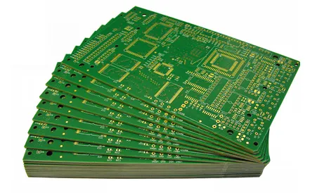
Introduction
Laser drilling has become essential in PCB manufacturing for creating precise microvias in high-density interconnect boards. These small apertures, often under 150 microns in diameter, enable compact designs for electronics like smartphones and medical devices. However, laser drilling defects PCB processes can lead to reliability issues if not managed properly. Common problems include heat-affected zones and tapered holes that compromise plating quality and signal integrity. This guide provides factory-driven insights into identifying and resolving these laser drilling problems. Electric engineers will find practical troubleshooting steps aligned with industry standards to improve yield and performance.
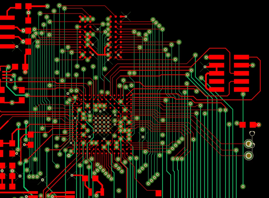
Understanding Laser Drilling in PCB Manufacturing
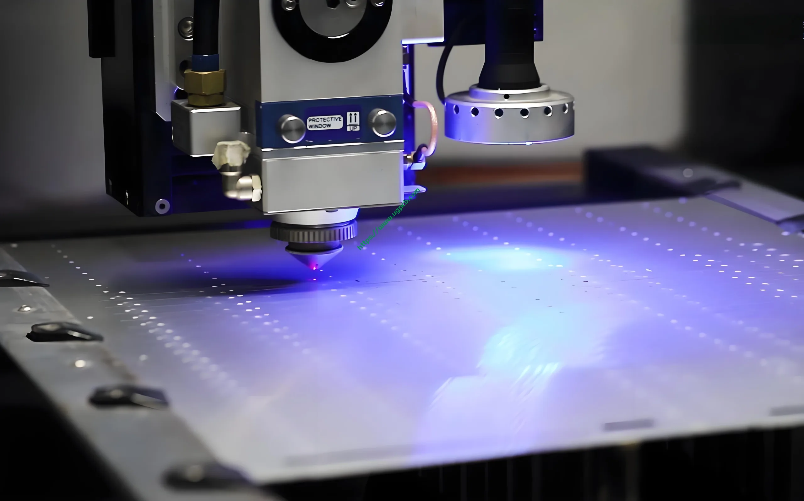
Laser drilling uses focused beams to ablate dielectric materials and copper layers selectively. CO2 lasers excel at removing resins due to high absorption at 9.3 to 10.6 microns wavelength, while UV lasers offer cleaner cuts with minimal thermal damage through photochemical ablation. Microvia defects arise when process parameters fail to match material properties, leading to inconsistencies in hole geometry. These defects matter because they affect subsequent steps like desmear, plating, and reliability under thermal cycling. In high-volume production, even minor laser drilling problems can increase scrap rates and delay shipments. Adhering to standards like IPC-6016 ensures vias meet performance criteria for high-density boards.
Common Causes of Laser Drilling Defects
Laser drilling defects stem from interactions between beam parameters, material composition, and equipment calibration. Excessive pulse energy can vaporize material unevenly, creating a wide heat-affected zone where resins char or delaminate. Beam focus misalignment causes tapered holes, with entry diameters larger than exits due to Gaussian beam divergence. Debris from ablation often redeposits as recast layers, roughening walls and trapping gases during plating. Material variability, such as inconsistent glass transition temperatures in laminates, exacerbates these issues under repeated laser passes. Factory data shows that unoptimized parameters account for over half of microvia rejects in initial runs.
Poor alignment between drill targets and copper pads leads to offset vias, compromising electrical connections. In stacked microvias, cumulative errors amplify into open circuits after assembly. Environmental factors like humidity affect resin ablation rates, causing incomplete penetration or blowback. These mechanisms highlight the need for precise process control in PCB manufacturing troubleshooting.
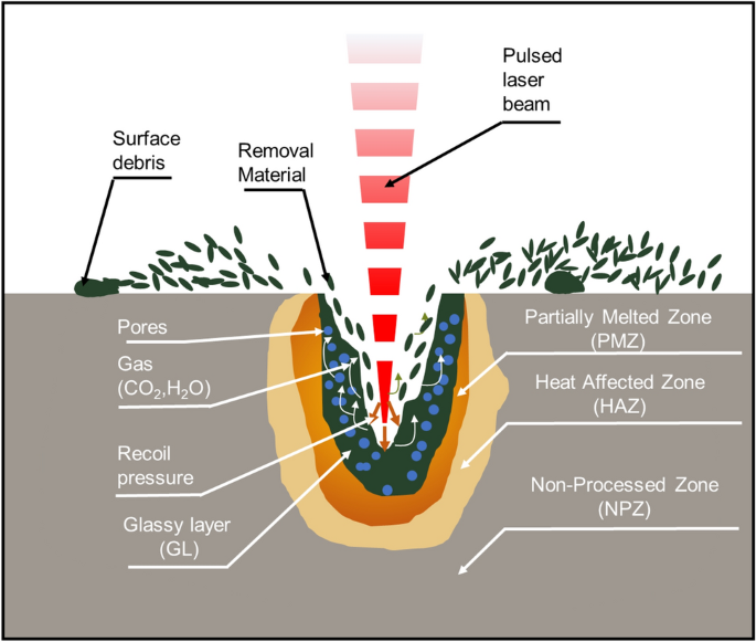
Key Laser Drilling Defects and Their Characteristics
Excessive Heat-Affected Zone (HAZ)
The heat-affected zone appears as darkened or carbonized rings around vias, weakening interlayer adhesion. High thermal input melts fibers and resins, forming microcracks that propagate under stress. UV lasers minimize HAZ compared to CO2 due to shorter wavelengths and cold ablation. Cross-sections reveal HAZ widths exceeding 10 microns as unacceptable per IPC-A-600 acceptability criteria. This defect reduces board reliability in reflow soldering. Engineers observe it via optical microscopy before desmear.
Tapered or Conical Holes
Taper manifests as a conical profile, with top diameters 20 to 30 percent larger than bottoms. Beam defocus or excessive depth-to-diameter ratios cause progressive widening. This geometry hinders uniform plating, leading to voids at via bottoms. Standards like IPC-6012 specify maximum taper angles for rigid boards to ensure plating coverage. Factories measure taper using automated optical inspection systems post-drill. Correcting it prevents barrel cracks in reliability tests.
Debris, Recast, and Resin Smear
Debris buildup includes molten particles that resolidify, creating rough walls prone to plating defects. Resin smear coats copper pads, blocking electroless seed layers. Inadequate assist gas flow fails to evacuate ejecta, worsening recast layers up to several microns thick. Plasma desmear removes smear but cannot fix severe debris. Microvia defects like these cause high-resistance vias or opens. SEM imaging confirms wall roughness exceeding Ra 2 microns as problematic.
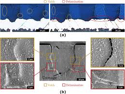
Wall Roughness and Voids
Rough via walls from uneven ablation trap air during plating, forming voids that weaken copper barrels. Stacked microvias amplify this, as bottom roughness propagates upward. Material fillers like silica affect ablation thresholds, leading to fibrous residues. Post-drill cleaning with permanganate etch smooths walls but requires parameter tuning. IPC-6016 guidelines for HDI boards mandate smooth walls for electroplating integrity. Voids appear in X-ray after fill, signaling upstream laser issues.
Practical Troubleshooting and Best Practices
Start troubleshooting with process data logs, correlating defect rates to laser parameters like fluence, repetition rate, and scan speed. Reduce HAZ by lowering peak power and using shorter pulses, targeting 1 to 5 J/cm2 for resins. For taper, calibrate galvo scanners daily and limit aspect ratios to 1:1 for blind vias. Implement assist gases like nitrogen at 10 to 20 psi to flush debris, improving hole cleanliness. Factories achieve 99 percent yield by running design-of-experiments on new stacks.
Material selection plays a key role; choose laser-drillable dielectrics with low ablation thresholds per IPC-2226 design standards. Pre-treat surfaces with plasma to enhance uniformity. Post-drill, verify geometry with automated metrology before desmear. Desmear processes must balance etch rates to avoid over-etching copper. Monitor plasma etch endpoints via optical emission spectroscopy. Regular maintenance of optics prevents beam profile degradation.
Integrate inline monitoring like acoustic emission sensors to detect anomalies real-time. For microvia defects, cross-section sample 1 percent of panels per lot, analyzing via IPC-A-600 class criteria. Train operators on parameter windows for specific materials. Collaborate with design teams to stagger vias, reducing stacking risks. These steps align factory processes with standards, minimizing laser drilling problems.
Inspection Methods for Laser Drilling Quality
Optical profilometry quantifies taper and roughness non-destructively. Cross-sectioning via focused ion beam reveals internal defects like microcracks. Electrical testing post-plating flags high-resistance vias from poor walls. Ultrasonic scanning detects delamination from HAZ. Factories standardize IPC-6016 qualification tests, including thermal shock cycles. Early detection prevents downstream failures.
Conclusion
Troubleshooting laser drilling defects PCB requires systematic control of parameters, materials, and processes. Addressing HAZ, taper, debris, and roughness ensures reliable microvias in demanding applications. Factory-driven best practices, backed by standards like IPC-6016 and IPC-A-600, boost yields and reduce rework. Electric engineers can apply these insights to optimize production lines. Consistent implementation leads to higher-quality boards and faster time-to-market. Prioritize data-driven adjustments for long-term success in PCB manufacturing troubleshooting.
FAQs
Q1: What are the most common laser drilling defects PCB?
A1: Common laser drilling defects PCB include excessive heat-affected zones, tapered holes, debris buildup, and rough walls leading to plating voids. These arise from mismatched laser parameters or material properties. Factories mitigate them through optimized fluence and assist gases. Cross-section analysis per IPC-A-600 confirms acceptability. Addressing them early improves HDI reliability.
Q2: How can manufacturers fix microvia defects from laser drilling problems?
A2: To fix microvia defects, calibrate beam focus to minimize taper and use UV lasers for cleaner ablation. Plasma desmear removes resin smear effectively. Verify wall roughness below 2 microns before plating. Standards like IPC-6016 guide acceptance criteria. Process tuning via DOE reduces recurrence in production.
Q3: What causes heat-affected zone in laser drilling PCB manufacturing troubleshooting?
A3: Heat-affected zone results from high thermal input vaporizing resins unevenly, causing charring and delamination. CO2 lasers produce larger HAZ than UV due to wavelength absorption. Optimize pulse energy and speed to limit it under 10 microns. Assist gases aid evacuation. IPC-6012 specifies limits for rigid boards.
Q4: Why do voids occur in laser-drilled microvias during plating?
A4: Voids form from rough walls trapping gases, often due to inconsistent ablation or debris. Laser drilling problems like fibrous residues exacerbate this. Proper desmear and plating agitation resolve it. Staggered designs per IPC-2226 reduce stacking risks. Inline inspection catches issues pre-plating.
References
IPC-6016D — Qualification and Performance Specification for High Density Interconnect (HDI) Printed Boards. IPC, 2018
IPC-A-600K — Acceptability of Printed Boards. IPC, 2020
IPC-6012E — Qualification and Performance Specification for Rigid Printed Boards. IPC, 2017