Introduction
Sequential lamination represents a critical process in manufacturing high-density interconnect (HDI) printed circuit boards (PCBs), enabling the creation of complex multilayer structures with blind and buried vias. This technique involves building the board layer by layer, laminating subcomposites sequentially to achieve precise control over layer stacking and via formation. However, the process introduces unique challenges, including delamination, resin cracks, and voids, which can compromise board reliability and performance. These defects often stem from material interactions, process variations, or environmental factors during fabrication. Electric engineers must understand PCB delamination causes, sequential lamination resin crack prevention strategies, and methods to minimize void formation in PCB to ensure robust designs. Addressing these issues early in the manufacturing workflow prevents costly rework and field failures in demanding applications like telecommunications and aerospace electronics.

Factory-driven insights emphasize the need for tight process controls, as even minor deviations can propagate through multiple lamination cycles. By aligning fabrication parameters with material specifications, engineers can mitigate risks associated with thermal stresses and resin flow dynamics. This article explores the underlying mechanisms, root causes, and proven best practices, drawing on established industry standards for guidance.
What Is Sequential Lamination and Why It Matters
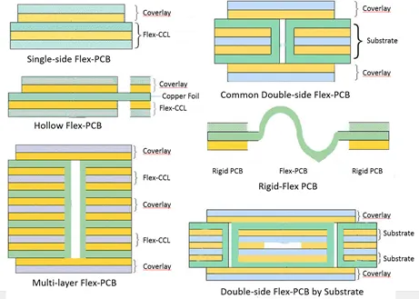
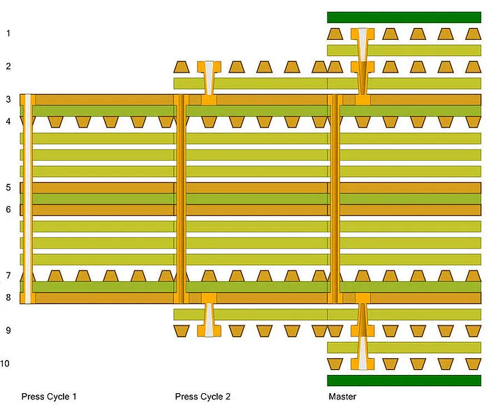
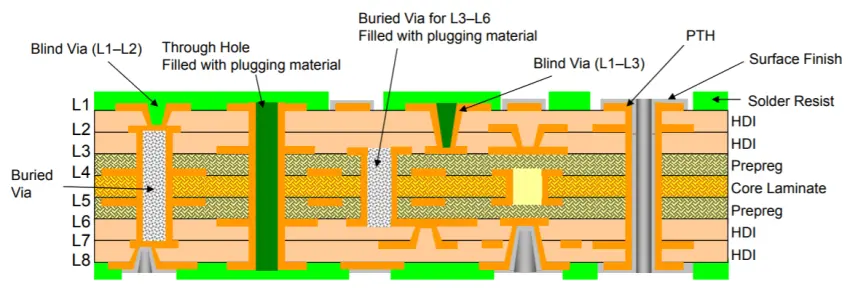
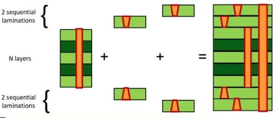
Sequential lamination builds PCBs by repeatedly stacking cores, prepregs, and copper foils in a controlled sequence, unlike traditional all-at-once lamination for simpler multilayers. Each cycle involves precise alignment, lamination under heat and pressure, and subsequent processing for vias or imaging. This method supports advanced HDI features, such as stacked microvias, by allowing intermediate layers to be drilled and plated before final buildup. The process demands high material compatibility and process repeatability to maintain interlayer integrity across 10 or more layers.
In high-performance electronics, sequential lamination matters because it enables denser routing, shorter signal paths, and better impedance control, critical for high-speed signals in 5G modules or servers. Yet, the iterative nature amplifies defect risks, as cumulative stresses from multiple heat-pressure cycles can lead to failures not seen in standard multilayers. PCB delamination causes become more pronounced here due to repeated exposure to thermal gradients. Engineers rely on this process for boards exceeding 20 layers, where conventional methods fall short in via reliability.
Adherence to standards like IPC-6012E ensures qualification for rigid printed boards, specifying performance criteria for lamination quality. Factory experience shows that sequential lamination reduces overall board thickness while improving thermal management, but only if defects like voids are controlled. For electric engineers, mastering this process translates to higher yields and reliable prototypes transitioning to production.
Understanding the Key Defects in Sequential Lamination
PCB Delamination Causes
Delamination occurs when adhesive bonds between copper foil, prepreg, or core layers separate, often visible as blisters or separations in cross-sections. Primary PCB delamination causes include moisture absorption in laminates, leading to steam expansion during high-temperature lamination. Contamination from handling or inadequate surface preparation disrupts resin wetting, preventing uniform bonding. Thermal expansion mismatches between materials exacerbate separation under pressure cycles.
In sequential lamination, low copper density on inner layers creates resin-rich areas prone to delamination, as uneven flow leaves weak interfaces. Improper lamination parameters, such as excessive ramp rates or insufficient dwell time, fail to achieve full consolidation. Factory data correlates these issues with panel warpage, where bowed substrates misalign during stacking. IPC-A-600K outlines acceptability criteria, classifying delamination by depth and extent to guide inspections.
Engineers should note that repeated lamination cycles compound stresses, making early detection via C-scan ultrasound essential. Addressing PCB delamination causes requires holistic process audits, from material incoming to final press.
Sequential Lamination Resin Crack Prevention Insights
Resin cracks manifest as fractures in the cured epoxy matrix, typically along the Z-axis, compromising dielectric integrity and via reliability. These arise from excessive shear during lamination, especially in thick prepregs under high pressure. Thermal shock from rapid heating causes differential expansion, cracking brittle resins with low glass transition temperature (Tg). In sequential builds, prior cycle residues or incomplete cures propagate cracks into subsequent layers.
Void formation in PCB often accompanies cracks if trapped gases expand under heat. Prevention hinges on material selection with matched coefficients of thermal expansion (CTE) and high fracture toughness. Controlled ramp-up profiles, below 2 degrees Celsius per minute, minimize stress gradients. Sequential lamination resin crack prevention also involves optimizing resin content in prepregs, typically 50 to 60 percent, to balance flow and strength.
Factory best practices include post-lamination bakes to relieve residual stresses before drilling. J-STD-020E provides moisture sensitivity classifications, informing preconditioning to avert crack initiation. Regular peel strength tests per IPC-TM-650 validate process robustness.
Void Formation in PCB During Sequential Lamination
Voids are air or gas pockets trapped between layers, reducing bond strength and creating paths for contaminants. Void formation in PCB stems from inadequate vacuum during layup, allowing air entrapment, or outgassing from volatile resins. Insufficient pressure fails to squeeze out gases, while aggressive heat ramps volatilize moisture prematurely. In sequential processes, microvias from prior steps act as traps if not cleared properly.
Resin starvation in high-copper areas leaves unfilled gaps, evolving into voids post-cure. Detection via acoustic microscopy reveals voids larger than 5 percent of layer thickness as rejects. Prevention strategies focus on full vacuum chambers and staged pressure application, starting low and ramping to full consolidation.
These defects interconnect; a void can nucleate cracks under thermal cycling, leading to delamination. Standards like IPC-6012E limit void sizes to ensure reliability.
Best Practices for Prevention and Process Optimization
Effective sequential lamination demands integrated controls across material handling, layup, pressing, and inspection. Begin with moisture management: bake laminates and prepregs at 120 to 150 degrees Celsius for 4 to 8 hours to desorb water below 0.25 percent content. Select FR-4 or higher-Tg resins with low Z-axis CTE for multilayer stability, ensuring compatibility across suppliers.
Layup precision prevents misalignment, a precursor to uneven pressure and voids. Use automated optical registration and copper balancing, maintaining 40 to 60 percent density per layer to promote uniform resin flow. Lamination cycles should follow validated profiles: gradual heat to 180 to 220 degrees Celsius, 200 to 400 psi pressure, and 60 to 120 minutes dwell.
Post-lamination, perform warpage checks and cross-section analysis to quantify defects early. Sequential lamination resin crack prevention improves with filled vias in prior layers, distributing stresses. Implement statistical process control, tracking peel strength above 4 pounds per inch.
For void formation in PCB, enhance vacuum to below 20 torr and use breather fabrics for gas escape. Factory yields exceed 95 percent with these measures, per IPC-9121 troubleshooting guidelines.
Troubleshooting Sequential Lamination Defects
Diagnose issues systematically: review process logs for parameter excursions, then inspect via microscopy or X-ray. Delamination shows as horizontal separations; trace to moisture via weight gain tests. Resin cracks appear as white lines in dye-and-peel; correlate with Tg via DSC analysis.
Voids require SAM scanning; small ones under high-copper tie to resin content. Adjust by increasing prepreg sheets or switching styles. Rework options include re-lamination for early panels, but production favors prevention.
Document root causes in a Pareto chart to refine SPC limits. Electric engineers benefit from collaborating with fabricators on design for manufacturability (DFM) reviews.
Conclusion
Troubleshooting sequential lamination requires vigilance against PCB delamination causes, proactive sequential lamination resin crack prevention, and rigorous controls for void formation in PCB. By mastering material selection, process parameters, and inspections aligned with IPC standards, engineers achieve reliable HDI boards. Factory insights underscore the value of iterative validation, ensuring high yields and performance. Prioritize these practices to elevate your PCB manufacturing outcomes.
FAQs
Q1: What are the main PCB delamination causes in sequential lamination?
A1: Moisture absorption, thermal mismatches, contamination, and improper lamination parameters top the list. Moisture erupts as steam during heating, while contamination hinders resin adhesion. Low copper density leads to uneven flow, and rapid ramps induce stresses. Mitigate with baking, surface preparation, balanced copper designs, and validated press profiles for robust bonds.
Q2: How can engineers implement sequential lamination resin crack prevention?
A2: Select high-Tg materials with matched CTE, use controlled ramp rates under 2 degrees Celsius per minute, and ensure proper resin content in prepregs. Apply post-lamination stress-relief bakes and verify adhesion with peel tests per IPC-TM-650. Balance copper to avoid shear concentrations and consider filled vias to distribute Z-axis stresses.
Q3: What leads to void formation in PCB during lamination and how to avoid it?
A3: Trapped air, outgassing, moisture volatilization, and poor resin flow cause voids. Inadequate vacuum or pressure prevents consolidation. Avoid by achieving deep vacuum, using staged pressure application, optimizing ramp profiles, employing breather fabrics, and balancing copper to promote even resin distribution. Use acoustic scans to detect and correct early.
Q4: Why is process control critical for avoiding delamination in high-layer PCBs?
A4: Sequential builds amplify cumulative thermal and mechanical stresses, so parameter deviations propagate defects across cycles. Uniform, validated profiles ensure resin flow, consolidation, and bonding. Standards like IPC-6012E set performance benchmarks; adherence, SPC monitoring, and regular inspections yield reliable HDI performance and high production yields.
References
IPC-6012E — Qualification and Performance Specification for Rigid Printed Boards. IPC, 2017
IPC-A-600K — Acceptability of Printed Boards. IPC, 2020
J-STD-020E — Moisture/Reflow Sensitivity Classification. JEDEC, 2014
IPC-9121 — Troubleshooting for Printed Board Fabrication Processes. IPC, latest