Introduction
Stacked vias play a critical role in high-density interconnect (HDI) printed circuit boards, allowing vertical connections across multiple layers in compact designs. These structures enable finer pitch routing and smaller footprints essential for modern electronics like smartphones and servers. However, they introduce unique challenges in reliability, where failures such as cracks, delamination, and open circuits can compromise entire assemblies. Engineers often encounter these issues during production ramp-up or field returns, making stacked via failure analysis a key skill for maintaining product integrity. This guide provides a structured approach to identifying causes, performing analysis, and implementing solutions grounded in engineering principles. By addressing stacked via reliability issues proactively, teams can enhance PCB performance and reduce downtime.
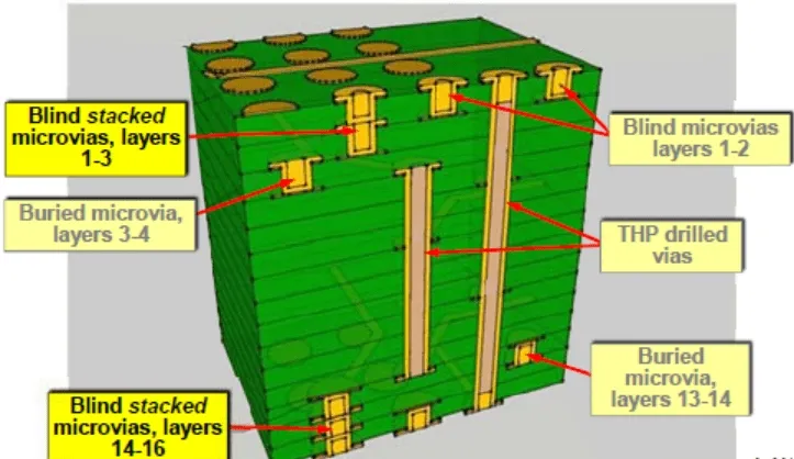
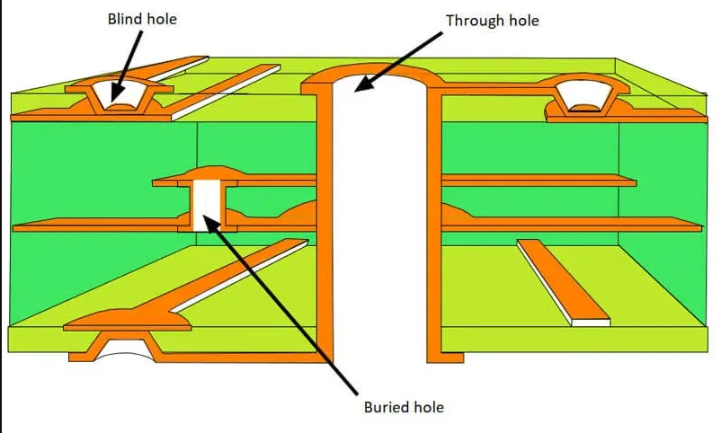
What Are Stacked Vias and Why Do They Matter?
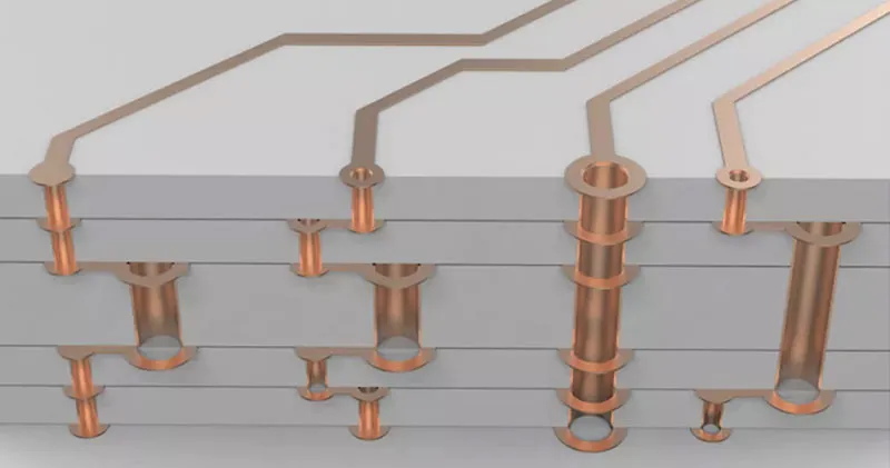
Stacked vias consist of multiple blind or buried vias aligned directly on top of each other, spanning several dielectric layers to form a continuous conductive path. Unlike staggered vias, which offset each via slightly for better stress distribution, stacked configurations minimize board area but concentrate mechanical loads. They are common in HDI PCBs built via sequential lamination processes, where each via layer is drilled, plated, and laminated individually. The relevance stems from their use in high-performance applications demanding dense interconnects, yet they amplify risks during thermal excursions common in soldering or operation. Stacked via reliability issues arise primarily from the cumulative effects of these stresses, potentially leading to field failures that affect yield and warranty costs. Understanding their structure helps engineers prioritize design trade-offs early.
Common Mechanisms Behind Stacked Via Failures
Thermal cycling induces shear stresses at via interfaces due to coefficient of thermal expansion (CTE) mismatches between copper plating and the surrounding dielectric resin. Repeated expansion and contraction cause fatigue, initiating microcracks that propagate under continued load. In stacked configurations, these stresses compound across layers, accelerating degradation compared to single vias. Manufacturing variations, such as drill smear residue or inconsistent plating thickness, further weaken barrel integrity. Delamination often follows, as interfacial adhesion fails under combined hygrothermal stress. Open circuits emerge when cracks sever the conductive path entirely.
Poor laser drilling alignment in microvia stacks leads to overhangs or voids at landings, compromising electrical continuity. Plating defects, including dog-boning or incomplete fill, create weak points susceptible to electromigration over time. IPC-TM-650 test methods highlight how these flaws manifest during accelerated life testing. Moisture absorption exacerbates issues by swelling dielectrics, promoting delamination at copper-resin boundaries. Engineers must consider these interactions holistically during stacked via failure analysis.
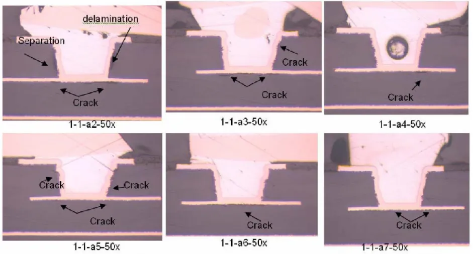
Detailed Failure Modes: Cracks, Delamination, and Open Circuits
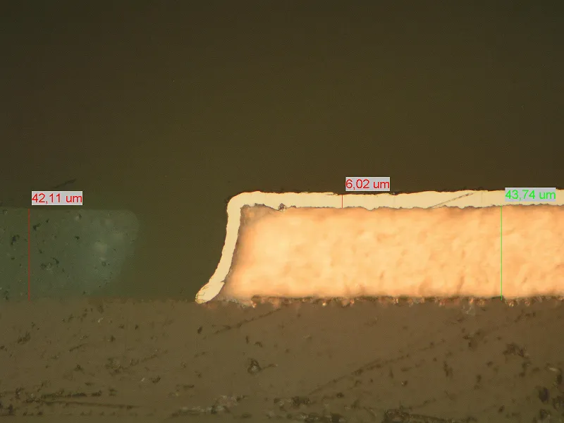
Stacked via cracks typically originate at the via corner or knee, where stress concentrations peak during flexure or temperature swings. Finite element analysis reveals higher strain in upper stack layers due to board warpage. Propagation follows the plated barrel, eventually bridging to adjacent layers. Delamination manifests as separation between via plating and dielectric, often visible in cross-sections after thermal shock. This mode links to surface contamination or inadequate plasma desmear, reducing peel strength. Resulting voids trap contaminants, hastening corrosion.
Open circuits represent the end-state of progressive damage, where resistance spikes indicate barrel discontinuity. Early detection via flying probe testing prevents assembly escapes. Stacked via delamination frequently pairs with cracking, as adhesive failure relieves stress but severs connections. Hygroscopic swelling in humid environments amplifies both, underscoring bake-out protocols pre-lamination. Reliability data from daisy-chain coupons correlate stack height to failure rates, guiding design limits.
Stacked Via Failure Analysis Techniques
Begin with non-destructive electrical testing using time-domain reflectometry to pinpoint opens or high-resistance segments. X-ray laminography reveals internal voids or cracks without sectioning. For deeper insight, perform cross-sectioning at suspect locations, polishing to 1 micron finish for optical microscopy. Scanning electron microscopy (SEM) with energy-dispersive X-ray spectroscopy identifies elemental composition at failure sites, distinguishing plating defects from thermal damage. Dye-and-peel tests quantify delamination extent per IPC-A-600 criteria.
Thermal profiling during analysis simulates operational conditions, monitoring resistance changes via IPC-TM-650 2.6.27 procedures. Acoustic microscopy detects subsurface delamination through ultrasound reflections. Combine these with Weibull analysis of coupon data to extrapolate field life. Document findings systematically to inform root cause and corrective actions.
Best Practices for Preventing Stacked Via Reliability Issues
Adhere to IPC-2226 guidelines for HDI stackups, limiting stacked vias to two levels maximum to distribute stress. Opt for staggered vias in non-critical nets to improve robustness without area penalty. Specify copper-filled vias for enhanced mechanical strength, particularly in outer layers. Maintain laser via aspect ratios below 1:1, ensuring clean drilling with optimized fluence. Select low-CTE resin systems matched to copper's expansion properties.
Process controls include plasma cleaning post-drill to remove smear, followed by electroless copper seed for uniform plating. Sequential lamination demands precise registration, verified via automated optical inspection. Implement via tenting or capping to shield from solder exposure. Pre-condition boards per JEDEC moisture sensitivity levels before reflow.
Qualification testing employs IPC-TM-650 2.6.27 D-coupons, subjecting stacks to 1000 thermal cycles from -40°C to 125°C while tracking resistance. Criteria include less than 10% increase and no opens. Warpage control below 0.75% per IPC-TM-650 2.4.22 prevents additional bending stress.
Troubleshooting Workflow for Stacked Via Problems
Assess symptoms: intermittent opens suggest cracking, stable high resistance points to plating voids, while thermal failures indicate delamination. Isolate via chains electrically, then thermally stress suspect sections. Cross-section multiple samples along the stack to map progression. Correlate with process data like drill hit rates or plating bath chemistry.
If cracks dominate, review CTE specs and cycle counts. Delamination calls for adhesion promoter audits. Open circuits warrant plating thickness verification via beta backscatter. Iterate designs with simulation, validating via accelerated tests. Track improvements through failure mode effects analysis.
Conclusion
Mastering stacked via troubleshooting demands integrating design, process, and test disciplines to mitigate inherent reliability risks. By recognizing mechanisms like CTE-driven cracks and delamination, engineers can deploy targeted solutions such as limited stacking and rigorous qualification. Standards like IPC-TM-650 provide proven frameworks for validation, ensuring robust performance. Proactive failure analysis not only resolves issues but elevates overall PCB quality. Apply these principles to sustain high yields and long-term dependability in demanding applications.
FAQs
Q1: What causes stacked via crack in PCBs during thermal cycling?
A1: Stacked via cracks stem from shear stresses due to CTE mismatch between copper and dielectric materials under temperature fluctuations. Fatigue accumulates over cycles, concentrating at via corners in multi-level stacks. Manufacturing factors like plating inconsistencies exacerbate propagation. Mitigate by limiting stack height and using filled vias, validated through IPC-TM-650 thermal cycling tests. Early detection via resistance monitoring prevents field failures.
Q2: How do you perform stacked via failure analysis for delamination?
A2: Stacked via delamination analysis starts with cross-sectioning and SEM inspection to visualize interfacial separation. Dye-and-peel quantifies affected area, while acoustic microscopy screens non-destructively. Correlate with moisture history and lamination parameters. Root causes often trace to poor desmear or resin flow issues. Improve adhesion via plasma treatment and low-CTE materials for reliability.
Q3: What are common stacked via reliability issues leading to open circuits?
A3: Open circuits in stacked vias arise from cracks severing the barrel or plating voids interrupting conductivity. Thermal stress and misalignment compound these in HDI builds. Electrical testing pinpoints locations, followed by X-ray for confirmation. Address via copper filling and aspect ratio controls per IPC-2226. Coupon testing ensures design margins against operational stresses.
Q4: How can engineers avoid stacked via open circuit during manufacturing?
A4: Prevent stacked via open circuits by optimizing drill-plating sequences and verifying registration accuracy. Use electroless copper for void-free barrels, tenting vias against contamination. Qualify with daisy-chain resistance checks post-lamination. Thermal preconditioning simulates reflow stresses early. These steps, aligned with IPC standards, minimize escapes and enhance yield.
References
IPC-TM-650 — Test Methods Manual. IPC, 2020
IPC-2226 — Design Standard for High Density Interconnects. IPC, 2018
IPC-6012DS — Qualification and Performance Specification for High Density Interconnect (HDI) Printed Boards. IPC, 2017