Why are BGA solder joint integrity and inspection so important for modern electronics?
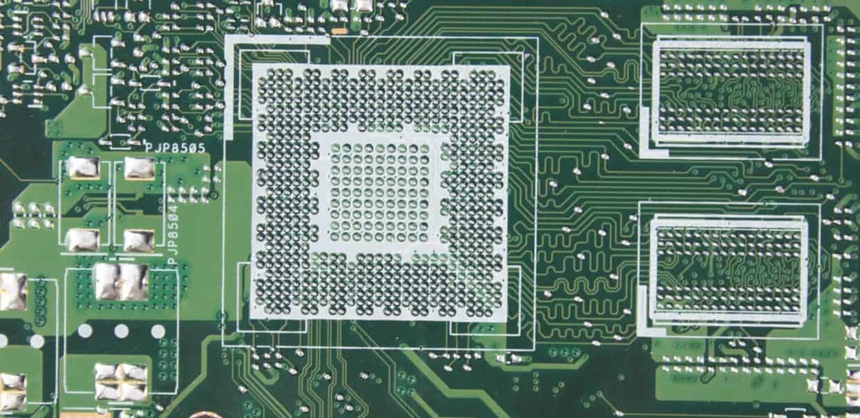
Ball Grid Array (BGA) components are fundamental to today's high-density electronics, enabling thousands of connections within a small space—ideal for sophisticated devices like microprocessors and GPUs. However, their design, which conceals numerous solder balls beneath the package, makes them particularly susceptible to invisible defects. These hidden flaws can severely compromise electrical performance or lead to complete system failure.
Common issues such as open circuits, unintended shorts, internal voids, and "head-in-pillow" (HIP) defects can cause anything from intermittent connectivity to critical overheating. For engineers, failing to identify these problems during manufacturing or testing can result in expensive reworks, product recalls, or damage to brand reputation. Consequently, X-Ray inspection becomes indispensable as it's the only dependable method to examine the solder joints beneath a BGA and pinpoint defects before they escalate.
What specific BGA solder joint defects can X-Ray inspection uncover?
Before delving into how X-Ray technology works, it's beneficial to understand the prevalent types of BGA solder joint defects. Recognizing these issues highlights the necessity for advanced inspection techniques beyond visual checks.
Open Circuits
An open circuit signifies a failure where a solder ball does not properly connect to its corresponding PCB pad. This can stem from insufficient solder paste, incorrect component placement, or thermal stress during reflow. The consequence is a complete disruption of electrical signal flow. In high-frequency designs, even a single open circuit can introduce significant signal integrity problems, leading to data corruption or system crashes.
Short Circuits
Shorts occur when excess solder creates an unintended bridge between adjacent solder balls. This can be caused by excessive solder paste volume or poorly designed SMT stencil. Shorts are particularly critical in power distribution networks, where they can induce overcurrent conditions, lead to localized overheating, or even result in component burnout. X-Ray detection of BGA shorts is crucial to prevent such severe failures.
Voids
Voids are small pockets of air or gas trapped within the solder joint, often caused by outgassing from flux during the reflow process or inadequate wetting. Significant voiding (e.g., more than 25% of the joint area) compromises both the mechanical strength and thermal conductivity of the connection. In power-intensive applications, extensive voids can drastically reduce heat dissipation, causing component junction temperatures to exceed safe operating limits.
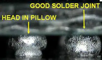
Head-in-Pillow (HIP) Defects
The "head-in-pillow" defect describes a condition where the solder ball and solder paste do not fully merge during reflow, creating a weak, unbonded, or intermittently connected interface. This often happens due to warpage of either the BGA package or the PCB under thermal stress. HIP defects are particularly challenging because they frequently cause intermittent failures, making them difficult to diagnose without advanced tools like X-Ray inspection.
How does X-Ray technology reveal these hidden BGA flaws?
Unlike surface-level inspection methods, X-Ray technology penetrates materials to expose the internal structure of BGA solder joints. This non-destructive testing technique uses X-rays to generate detailed two-dimensional (2D) or three-dimensional (3D) images of the hidden connections, making otherwise invisible defects apparent to engineers.
The Fundamentals of BGA X-Ray Systems
X-Ray inspection machines operate by directing high-energy X-rays through the assembled PCB. Denser materials, such as solder, absorb more X-rays and appear darker in the resulting image, while less dense areas like air pockets (voids) or gaps appear lighter. Modern X-Ray systems can achieve resolutions as fine as 1 micron, allowing them to pinpoint even minute anomalies in solder joints, even those with diameters as small as 0.3 mm. For BGA inspection, 2D X-Ray imaging and 3D Computed Tomography (CT) X-Ray are the primary techniques, each suited for different levels of detail and defect complexity.
2D X-Ray Imaging for Initial Defect Screening
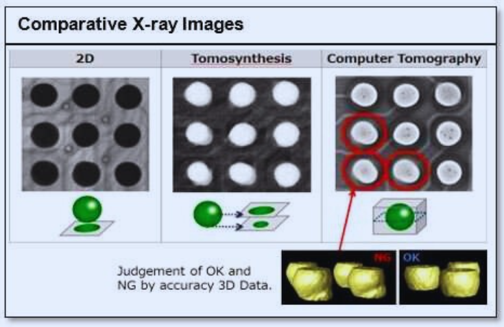
2D X-Ray imaging offers a rapid and cost-effective method for acquiring a top-down or angled view of BGA solder joints. It's effective for identifying clear issues like open circuits, shorts, and large voids. For example, a solder bridge will appear as an irregular dark mass connecting adjacent balls, while an open circuit might show as a distinct gap where solder should be. However, 2D X-Ray has limitations, particularly with overlapping structures or when precise depth information is needed, making it less ideal for complex issues like head-in-pillow defects.
3D CT X-Ray for Comprehensive Defect Analysis
3D CT X-Ray elevates inspection by constructing a complete three-dimensional model of the BGA assembly. By combining numerous 2D images taken from various angles, 3D CT can precisely map the location and nature of defects across all dimensions. This capability is crucial for accurately visualizing head-in-pillow defects, clearly showing the separation between the solder ball and paste in cross-sectional views. While more time-intensive and expensive, 3D CT is invaluable for critical applications such as aerospace or medical devices, where absolute reliability is paramount. Some systems can even quantify void percentages with high accuracy, ensuring compliance with industry standards like IPC-A-610.
What are the key advantages of integrating X-Ray inspection into manufacturing?
Implementing X-Ray inspection provides significant benefits for engineers focused on high-reliability or high-performance electronics manufacturing and testing.
● Non-Destructive Evaluation: X-Ray technology allows for internal solder joint assessment without causing any damage to the PCB, preserving valuable prototype board or production units.
● Early Defect Identification: Detecting flaws like voids or shorts during the manufacturing phase helps prevent costly field failures, reducing warranty claims and rework expenses.
● Process Refinement: Data from X-Ray inspections can reveal defect patterns, enabling engineers to optimize reflow profiles, solder paste deposition, or component placement accuracy. For instance, a slight reduction in peak reflow temperature could significantly mitigate warpage and HIP defects.
● Standard Compliance: X-Ray inspection helps ensure that assemblies meet rigorous industry standards such as IPC-A-610, which is frequently mandated for automotive or military-grade applications.
What challenges and best practices are associated with BGA X-Ray inspection?
While X-Ray inspection is a potent diagnostic tool, it comes with certain challenges. Understanding these limitations helps in setting realistic expectations and deciding when to complement X-Ray with other testing methods.
Common Challenges
The primary challenges include the cost and time investment required; high-end 3D CT systems can be very expensive, and detailed scans can slow down high-volume production. Interpretation complexity is another factor, as analyzing X-Ray images accurately often demands specialized training or advanced software to avoid misdiagnoses. Additionally, radiation safety requires X-Ray equipment to be operated within controlled environments, adding to operational overhead.
Recommended Best Practices
To maximize the efficacy of BGA X-Ray inspection:
● Select appropriate equipment: Opt for a 2D X-Ray system with at least 5-micron resolution for quick checks, or invest in a 3D CT system for critical, detailed analyses.
● Establish reference baselines: Create detailed X-Ray images of known good BGA joints under your specific production conditions for comparison.
● Ensure team proficiency: Provide thorough training for operators and engineers to accurately interpret X-Ray images, especially for subtle or nascent defects.
● Integrate with other tests: Combine X-Ray results with functional testing or thermal imaging to corroborate suspected defects.
● Systematic documentation: Maintain a comprehensive database of X-Ray findings to track defect trends, aiding in identifying root causes, such as inconsistent solder paste application.
Concluding thoughts on BGA reliability through X-Ray insights
BGA solder joint defects—including open circuits, shorts, voids, and head-in-pillow issues—pose significant threats to the performance and reliability of electronic devices. X-Ray inspection, with its unique capacity to visualize hidden problems beneath component packages, is an indispensable tool for engineers committed to achieving perfection in PCB assembly. Whether employing 2D imaging for rapid checks or 3D CT for in-depth analysis, this technology empowers early detection and resolution of issues, ultimately saving time, financial resources, and maintaining brand integrity. By thoroughly understanding the types of defects that affect BGAs and strategically applying X-Ray inspection techniques, engineers can ensure their designs adhere to the most stringent quality benchmarks. The next time you are diagnosing a board failure or refining a production line, remember the profound capability of X-Ray to reveal the secrets held within BGA solder joints.


