Introduction
High Tg PCBs are essential in modern electronics, especially for applications requiring enhanced thermal stability and reliable signal integrity. These boards, characterized by a high glass transition temperature, are often used in high-speed circuits where controlled impedance plays a critical role. For electrical engineers, mastering impedance control on high Tg PCBs ensures optimal performance in demanding environments like telecommunications, automotive systems, and industrial controls. This guide explores the relationship between high Tg materials, trace width, dielectric constant, and impedance matching. It provides practical insights into designing and manufacturing PCBs that meet stringent signal requirements while maintaining thermal resilience. By understanding these concepts, engineers can address challenges in high-speed designs and achieve consistent results in their projects.
What Is High Tg PCB and Why Controlled Impedance Matters
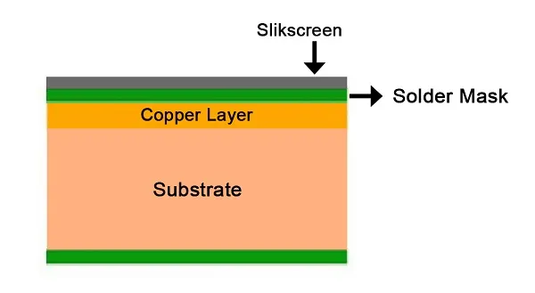
High Tg PCBs are printed circuit boards made with materials that have a high glass transition temperature, typically above 170 degrees Celsius. This property allows the board to withstand elevated temperatures without deforming or losing mechanical strength, making them ideal for applications exposed to harsh thermal conditions. The dielectric constant of these materials also influences their electrical performance, particularly in high-frequency circuits.
Controlled impedance is a design technique that ensures signal integrity by maintaining a consistent impedance value along transmission lines on the PCB. In high-speed digital and RF applications, mismatches in impedance can lead to signal reflections, crosstalk, and data loss. For high Tg PCBs, achieving controlled impedance is vital because they are often used in environments where signal accuracy cannot be compromised. Factors like trace width, dielectric thickness, and material properties directly affect impedance values. Engineers must prioritize these elements to prevent performance issues in critical systems.
Technical Principles of High Tg PCB Impedance Control
Role of Dielectric Constant in High Tg Materials
The dielectric constant, often denoted as Dk, measures a material's ability to store electrical energy in an electric field. For the high Tg PCB, materials with a stable and low dielectric constant are preferred in high-frequency applications to minimize signal delay and loss. Typically, high Tg laminates exhibit a Dk value tailored for specific impedance requirements. This property influences how signals propagate through the board and must be considered during the design phase to ensure high Tg PCB impedance matching.
When selecting a material, engineers must evaluate its dielectric constant across the operating frequency range. Variations in Dk can alter the characteristic impedance of traces, leading to potential mismatches. Standards such as IPC-4101E provide guidelines for choosing laminates with consistent electrical properties, ensuring reliability in high Tg PCB designs.
Impact of Trace Width on Controlled Impedance
Trace width is a fundamental factor in achieving high Tg PCB controlled impedance. Wider traces reduce impedance, while narrower traces increase it, assuming other parameters like dielectric thickness remain constant. In high-speed designs, engineers calculate trace width based on the desired impedance, often targeting values like 50 ohms for single-ended lines or 100 ohms for differential pairs.
The relationship between trace width and impedance is governed by the PCB stack-up and dielectric properties. Tools and formulas based on industry standards, such as those outlined in IPC-2221B, help determine appropriate dimensions. For high Tg PCBs, maintaining precise trace widths is crucial because thermal expansion can affect dimensional stability. Accurate fabrication processes ensure that trace geometries align with design specifications for consistent signal performance.
Dielectric Thickness and Stack-Up Design
Dielectric thickness between the trace and reference plane also influences impedance. Thinner dielectric layers increase capacitance, lowering impedance, while thicker layers have the opposite effect. In high Tg PCBs, stack-up design must balance thermal performance with electrical requirements. Engineers often use multilayer configurations to achieve controlled impedance while accommodating complex routing needs.
Standards like IPC-6012E emphasize the importance of maintaining uniform dielectric thickness during manufacturing to avoid impedance deviations. High Tg materials, with their enhanced thermal stability, help preserve layer integrity under heat stress, ensuring consistent electrical behavior. Proper stack-up planning is essential for high Tg PCB impedance matching, especially in high-frequency applications.
Thermal Effects on Impedance in High Tg PCBs
High Tg materials are designed to resist thermal deformation, but temperature changes can still impact impedance by altering the dielectric constant and trace dimensions. Elevated temperatures may cause slight shifts in material properties, affecting signal propagation. Engineers must account for these variations during design, particularly for applications in extreme environments.
Testing and simulation, guided by standards such as IPC-TM-650, allow engineers to predict how thermal stress influences impedance. High Tg PCBs mitigate some of these effects due to their robust composition, but careful material selection and design adjustments remain necessary for optimal performance.
Suggested Reading: High Tg PCB: Solving Heat Challenges in Demanding Electronics
Practical Solutions for High Tg PCB Impedance Control
Material Selection for Impedance Stability
Choosing the right high Tg material is the first step in achieving controlled impedance. Laminates with stable dielectric constants and low dissipation factors are ideal for high-speed circuits. Engineers should refer to specifications outlined in IPC-4101E to select materials that meet both thermal and electrical requirements. Consistency in material properties across production batches is critical to avoid impedance variations.
Calculating Trace Width for Target Impedance
To achieve high Tg PCB controlled impedance, trace width must be calculated based on the target impedance value and stack-up configuration. Equations and design tools aligned with IPC-2221B provide a reliable method for determining dimensions. For example, microstrip and stripline configurations require different calculations due to their distinct geometries. Collaboration with fabrication teams ensures that calculated widths are achievable within manufacturing tolerances.
Ensuring Uniform Dielectric Thickness
Uniform dielectric thickness across the PCB is vital for consistent impedance. Variations can lead to signal integrity issues, especially in high-frequency designs. Manufacturing processes must adhere to tolerances specified in IPC-6012E to maintain layer consistency. High Tg materials support this by resisting warping and delamination during thermal cycles, preserving dielectric integrity.
Impedance Matching Techniques
High Tg PCB impedance matching involves aligning the impedance of traces with connected components to minimize reflections. Techniques include adjusting trace widths, selecting appropriate dielectric materials, and using termination resistors where necessary. Differential pair routing also requires careful spacing and length matching to maintain impedance balance. Following design guidelines from IPC-2221B ensures that matching strategies are effective across various applications.
Testing and Validation
After manufacturing, impedance testing verifies that the PCB meets design specifications. Time-domain reflectometry and other methods, as described in IPC-TM-650, help measure actual impedance values and identify deviations. For high Tg PCBs, testing under thermal stress can reveal potential issues related to material behavior. Validation ensures that the board performs reliably in its intended application.
Troubleshooting Common Impedance Issues in High Tg PCBs
Impedance mismatches in high Tg PCBs often stem from manufacturing inconsistencies or design oversights. Uneven trace widths, caused by etching variations, can alter impedance values. Engineers should inspect fabrication reports to confirm compliance with tolerances outlined in IPC-A-600K. Dielectric thickness variations are another common issue, resolvable by enforcing strict process controls during lamination.
Thermal expansion, though minimized in high Tg materials, can still affect trace geometries in extreme conditions. Simulating thermal effects during the design phase helps predict and mitigate such problems. If mismatches occur, adjusting termination strategies or revising stack-up configurations may restore signal integrity. Consistent reference to industry standards ensures that troubleshooting efforts align with best practices.
Conclusion
Mastering high Tg PCB impedance control is essential for electrical engineers working on high-speed and thermally demanding applications. By understanding the interplay of dielectric constant, trace width, and stack-up design, professionals can achieve reliable signal integrity. High Tg materials provide the thermal stability needed for challenging environments, but precise design and manufacturing are equally important. Adhering to established standards and employing practical solutions ensures consistent performance. This guide offers actionable insights to help engineers navigate the complexities of high Tg PCB controlled impedance and deliver robust circuit designs.
FAQs
Q1: How does the dielectric constant affect high Tg PCB controlled impedance?
A1: The dielectric constant, or Dk, influences signal propagation speed and impedance in high Tg PCBs. A lower Dk reduces impedance for a given trace width and dielectric thickness, improving high-frequency performance. Engineers must select materials with stable Dk values to maintain consistency, ensuring signal integrity in demanding applications as per industry guidelines.
Q2: What factors determine high Tg PCB trace width for impedance control?
A2: High Tg PCB trace width is determined by target impedance, dielectric thickness, and material properties. Wider traces lower impedance, while narrower ones increase it. Calculations based on standard equations help achieve desired values. Stack-up design and manufacturing tolerances also play a role in maintaining accuracy during production.
Q3: Why is high Tg PCB impedance matching critical for high-speed designs?
A3: High Tg PCB impedance matching prevents signal reflections and crosstalk in high-speed circuits. Mismatches disrupt data transmission, causing errors. Matching trace impedance with components and using consistent dielectric properties ensures reliable performance. This is especially vital in telecommunications and automotive systems with stringent signal requirements.
Q4: How can engineers ensure consistent high Tg PCB dielectric constant during design?
A4: Engineers can ensure a consistent high Tg PCB dielectric constant by selecting materials with stable properties across frequencies, as guided by industry standards. Collaborating with fabricators to verify material batches and testing under operating conditions helps maintain uniformity. Proper documentation of specifications prevents deviations in production.
References
IPC-4101E — Specification for Base Materials for Rigid and Multilayer Printed Boards. IPC, 2021.
IPC-2221B — Generic Standard on Printed Board Design. IPC, 2012.
IPC-6012E — Qualification and Performance Specification for Rigid Printed Boards. IPC, 2020.
IPC-A-600K — Acceptability of Printed Boards. IPC, 2020.
IPC-TM-650 — Test Methods Manual. IPC, Current Revision.