Introduction
For electronic hobbyists venturing into printed circuit board design, achieving higher functionality in smaller spaces is a common goal. As devices shrink and components multiply, PCB density becomes a critical factor. This is where blind vias come into play as a powerful solution. These specialized connections allow designers to maximize space on multilayer boards by linking specific layers without passing through the entire board. In this guide, we explore blind vias for beginner PCB design, focusing on their role in enhancing PCB density vias. We will cover their definition, importance, design principles, and practical applications. Whether you are working on a compact gadget or a complex project, understanding how to use blind vias in PCB design can elevate your skills and help create efficient layouts with smart via solutions design.
What Are Blind Vias and Why Do They Matter
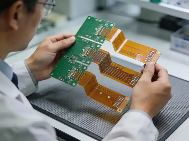
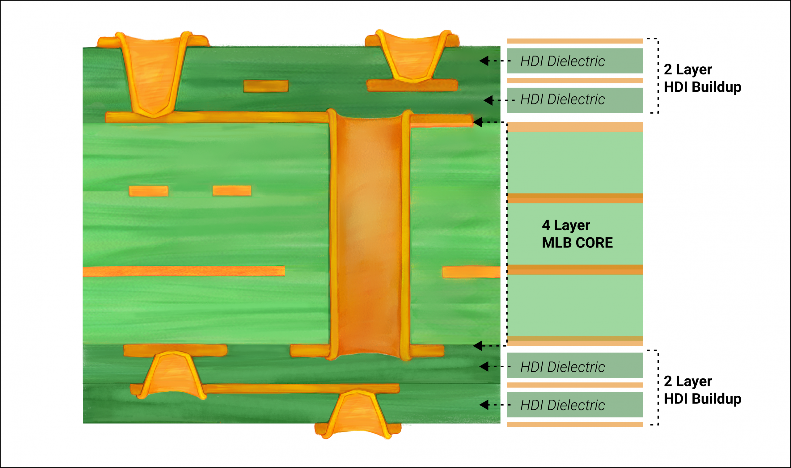
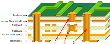
Blind vias are a type of interconnection in multilayer PCBs that connect an outer layer to one or more inner layers without extending through the entire board thickness. Unlike through hole vias, which span all layers, blind vias are only visible on one side of the board, making them ideal for high density designs. They are often used in applications where space is limited, such as smartphones, wearables, and other compact electronics.
Their importance lies in their ability to increase PCB density vias by freeing up space on the opposite side of the board. This allows for more components or routing options. For hobbyists, incorporating blind vias into beginner PCB design can significantly improve layout efficiency. They also support finer pitch components, which are common in modern electronics, by providing shorter signal paths and reducing interference. Understanding via solutions design with blind vias can transform how you approach complex projects.
Technical Principles of Blind Vias in PCB Design
Blind vias are created through a controlled depth drilling process, typically using laser technology for precision. This method ensures the via reaches only the intended inner layer without penetrating further. After drilling, the via is plated with copper to establish electrical conductivity between the connected layers. The process requires careful planning during the design phase to align with manufacturing capabilities.
From an engineering perspective, blind vias contribute to PCB density vias by reducing the number of through holes that occupy space across all layers. This selective connectivity minimizes signal path lengths, which can improve electrical performance by lowering inductance and capacitance. For beginner PCB design, it is crucial to note that blind vias are often used in conjunction with high density interconnect technology, which focuses on packing more functionality into smaller areas.
The design of blind vias must adhere to specific guidelines to ensure reliability. According to industry standards like IPC-6012E, the aspect ratio of the via, which is the ratio of depth to diameter, should be carefully considered to avoid manufacturing defects. A typical recommendation is to keep the aspect ratio below a certain threshold to ensure proper plating and structural integrity.
Related Reading: Blind Vias in PCB Design: Optimizing High-Density Boards

Benefits and Challenges of Using Blind Vias
Implementing blind vias in PCB design offers several advantages for hobbyists aiming to enhance PCB density vias. First, they allow for more compact layouts by freeing up space on the opposite board side. This is particularly useful when working with fine pitch components or ball grid array packages that require dense routing. Second, blind vias can improve signal integrity by shortening connection paths, reducing noise in high speed circuits.
However, there are challenges to consider in beginner PCB design. The manufacturing process for blind vias is more complex than for standard through holes, often requiring advanced equipment like laser drills. This can increase production costs and may not be feasible for all hobbyist budgets. Additionally, designing with blind vias demands precise layer alignment and stackup planning to avoid connectivity issues. Hobbyists must ensure their design software supports blind via specifications and that their chosen fabrication process can handle such features.
Practical Tips for Using Blind Vias in PCB Design
For electronic hobbyists looking to integrate blind vias into their projects, following best practices is essential for successful via solutions design. Start by understanding your project requirements. If your design involves multilayer boards with space constraints or high speed signals, blind vias could be a suitable choice. Evaluate whether the added complexity and cost align with your goals.
When planning how to use blind vias in PCB design, begin with a clear layer stackup. Define which layers need to connect via blind vias and ensure the connections are necessary for density or performance. Use design software that allows you to specify blind via parameters, such as depth and diameter, to match manufacturing capabilities. Refer to guidelines from standards like IPC-A-600K for acceptable via dimensions and tolerances to ensure reliability.
Collaboration with your fabrication partner is also critical. Confirm their ability to produce blind vias and ask for their design rules, such as minimum via size and aspect ratio limits. For beginner PCB design, start with simpler blind via configurations, avoiding overly complex stackups until you gain experience. Test your design with small prototype runs to identify potential issues before full production.
Related Reading: Through-Hole Vias: Essential Connections in Multilayer PCB Design
Common Applications of Blind Vias for Hobbyists
Blind vias are widely used in scenarios where PCB density vias are a priority. For hobbyists, they are particularly relevant in projects involving compact electronics. Consider a wearable device, such as a fitness tracker, where space is limited, and multiple components must fit on a small board. Blind vias can connect surface layers to inner signal layers without occupying space on the bottom side, allowing for additional component placement.
Another application is in high speed communication projects, like custom USB or wireless modules. Here, blind vias help maintain signal integrity by minimizing path lengths between layers. Hobbyists working on drone controllers or IoT devices can also benefit from via solutions design using blind vias to achieve tighter layouts without sacrificing performance. These examples highlight how blind vias can be a game changer in beginner PCB design for modern electronics.
Troubleshooting Blind Via Designs
Even with careful planning, issues can arise when using blind vias in PCB design. One common problem is misalignment during manufacturing, where the via does not connect to the intended layer. This can result from errors in stackup design or fabrication tolerances. To avoid this, double check your layer definitions and ensure they align with the manufacturer's capabilities.
Another issue is poor plating within the via, leading to weak electrical connections. This often stems from an improper aspect ratio or inadequate cleaning during fabrication. Adhering to standards like IPC-6012E for via design specifications can help mitigate such risks. For hobbyists, it is advisable to include test points in your design to verify connectivity after production. If problems persist, consult with your fabrication partner to adjust the design or process parameters.
Conclusion
Blind vias offer a valuable solution for electronic hobbyists seeking to enhance PCB density vias in their projects. By connecting specific layers without spanning the entire board, they enable more compact and efficient designs, making them ideal for modern, space constrained electronics. Understanding how to use blind vias in PCB design can significantly elevate your skills as a beginner in PCB design. While they come with challenges like increased manufacturing complexity, careful planning and adherence to industry standards can ensure success. With the right approach to via solutions design, you can unlock new possibilities in your hobbyist projects, creating layouts that are both functional and innovative. Dive into blind vias and take your PCB designs to the next level.
FAQs
Q1: What are blind vias, and how do they help with PCB density vias?
A1: Blind vias are connections in multilayer PCBs that link an outer layer to inner layers without passing through the entire board. They help increase PCB density vias by freeing up space on the opposite side, allowing more components or routing. This is especially useful for hobbyists designing compact devices with limited board area.
Q2: Can beginners in PCB design easily use blind vias in their projects?
A2: Yes, beginners in PCB design can use blind vias, but it requires careful planning. Start with simple multilayer designs and ensure your software supports blind via specifications. Check with your fabrication partner for their capabilities. Following standards like IPC-6012E helps ensure reliability in beginner PCB design.
Q3: What should I consider when learning how to use blind vias in PCB design?
A3: When learning how to use blind vias in PCB design, focus on layer stackup planning and via specifications like depth and diameter. Verify manufacturing limits with your fabricator. Consider the cost and complexity, and start with small prototypes to test your via solutions design before scaling up.
Q4: Are there specific standards for via solutions design using blind vias?
A4: Yes, standards like IPC-6012E and IPC-A-600K provide guidelines for via solutions design, including blind vias. They cover aspects like aspect ratio, plating quality, and tolerances. Adhering to these ensures manufacturability and reliability, which is crucial for hobbyists experimenting with high density PCB layouts.
References
IPC-6012E — Qualification and Performance Specification for Rigid Printed Boards. IPC, 2020.
IPC-A-600K — Acceptability of Printed Boards. IPC, 2020.