Introduction
In PCB design, selecting the right type of through-hole is a critical decision that impacts functionality, manufacturability, and cost. Plated through-holes (PTH) enable electrical interconnections between layers, while non-plated through-holes (NPTH) serve purely mechanical roles. Engineers often face PCB design decisions on whether to specify NPTH to optimize for specific applications. Understanding non-plated through hole usage helps avoid unnecessary complexity and expenses. This article explores NPTH applications, their advantages, and scenarios where they excel, particularly in cost-effective PCB solutions. By the end, you will know precisely when to incorporate NPTH for reliable performance.
What Are Non-Plated Through-Holes?
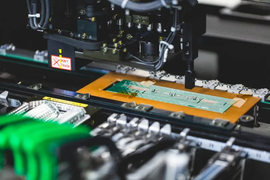
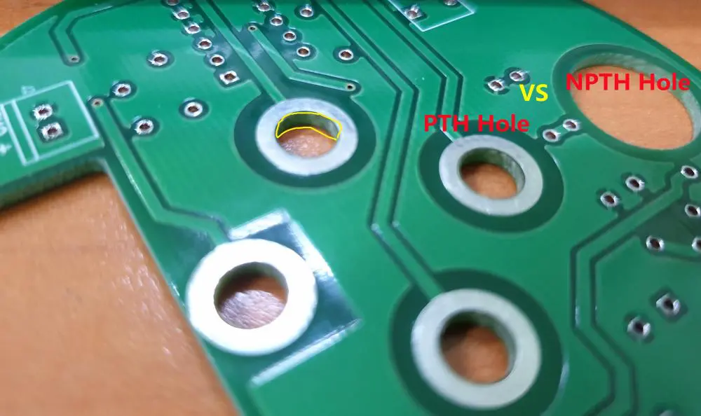
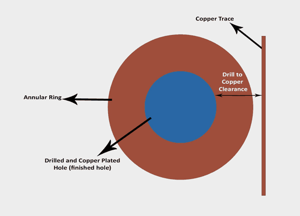
Non-plated through-holes, or NPTH, are drilled openings that extend completely through the PCB substrate without any copper plating on the barrel walls. Unlike PTH, which receive electroless copper deposition followed by electroplating to form conductive paths, NPTH remain as bare dielectric holes. This absence of plating makes NPTH ideal for non-electrical functions. Manufacturers drill NPTH using standard mechanical or laser processes, followed by any necessary deburring. The simplicity of NPTH construction aligns well with basic board types like single-layer PCB designs. Engineers specify NPTH in drill files separately from PTH to ensure proper fabrication routing.
Key Differences Between PTH and NPTH
PTH feature a continuous copper barrel that connects copper traces across layers, enabling via or component lead conductivity. NPTH lack this plating, so they isolate layers electrically and focus on structural support. Fabrication tolerances differ significantly; PTH demand tighter drill accuracy due to plating buildup, while NPTH allow more variation. Aspect ratios for NPTH can exceed those of PTH since no plating voids or cracks are a concern. In design software, NPTH pads, if present, do not connect to nets, preventing accidental electrical paths. These distinctions guide PCB design decisions toward NPTH when conductivity is unnecessary.
NPTH Applications in Modern PCB Designs
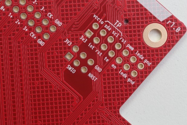
NPTH find primary use in mechanical fastening, such as screw mounting holes for securing boards to enclosures or chassis. Tooling holes represent another key NPTH application, aiding panelization, fiducial alignment, and automated handling during assembly. In edge connectors or card slots, NPTH provide precise slots without risking short circuits from plating. For prototypes or low-volume runs, NPTH support fixtures and test jigs effectively. Even in multilayer boards, isolated NPTH handle heat sink mounting where thermal conduction through the barrel is undesired. Selecting non-plated through hole usage here streamlines production without compromising mechanical integrity.
Advantages of NPTH for Cost-Effective PCB Solutions
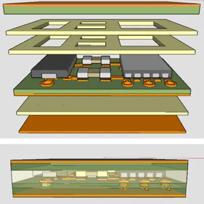
Choosing NPTH reduces manufacturing costs by eliminating the plating cycle, including desmear, activation, and electroplating steps. This leads to shorter lead times and lower material usage, ideal for cost-effective PCB solutions in budget-constrained projects. NPTH minimize risks like plating voids, barrel cracks, or resin smear, enhancing yield rates. In single-layer PCB, where interlayer connections are absent, all through-holes default to NPTH, simplifying the stackup. For double-layer PCB, NPTH for mounting complement PTH vias, balancing economy and function. Overall, NPTH support scalable designs without sacrificing essential performance.
Design Considerations for NPTH Implementation
Location matters greatly; place NPTH away from high-current traces to avoid drill breakout risks. Maintain adequate spacing from copper features, typically following generic design guidelines to prevent annular ring encroachment. Hole sizes for NPTH range based on fastener needs, with diameters oversized for clearance fits. Specify NPTH in separate drill files to direct fabricators correctly, ensuring no accidental plating. Aspect ratios up to 10:1 or higher suit NPTH since plating stresses are absent. Adhering to IPC-6012 qualification specifications guarantees NPTH meet performance criteria for rigid boards.
Best Practices for NPTH in Single-Layer and Double-Layer PCBs
In single-layer PCB, NPTH dominate as the only through-hole type, supporting component leads or mechanical anchors without electrical bridging. Double-layer PCB benefit from NPTH for peripheral mounting while reserving PTH for interlayer vias. Follow IPC-A-600 acceptability criteria to inspect NPTH for clean walls, free of burrs or debris. Optimize pad shapes around NPTH for solder mask definition, preventing exposure. Simulate mechanical stresses during design to confirm NPTH placement withstands vibration or torque. These practices ensure robust NPTH applications across board types.
Potential Challenges and Mitigation Strategies
One challenge with NPTH is drill wander in thicker boards, mitigated by precise CNC routing and pilot holes. Proximity to copper can cause breakout; enforce minimum edge-to-hole clearances per design rules. In high-volume production, ensure NPTH do not interfere with panel routing tabs. For double-layer PCB, mask NPTH properly to block solder wicking during wave soldering. Thermal expansion mismatches at NPTH sites require material selection considerations. Proactive design reviews address these, upholding reliability.
Case Insights from Common Engineering Scenarios
Consider a control panel PCB using double-layer construction; PTH handle signal routing, while NPTH secure DIN rail mounts. In single-layer PCB for power supplies, NPTH accommodate large standoffs without plating costs. Automotive prototypes leverage NPTH for vibration-resistant fixtures, passing shake tests. These examples highlight non-plated through hole usage in real-world PCB design decisions. Engineers report yield improvements of up to 5% by minimizing PTH count. Strategic NPTH integration proves versatile across sectors.
Conclusion
Non-plated through-holes offer engineers a straightforward, economical choice for mechanical needs in PCB design. Their applications span mounting, tooling, and alignment, excelling in single-layer PCB and supporting double-layer PCB efficiently. By prioritizing NPTH where electrical conduction is unneeded, teams achieve cost-effective PCB solutions without reliability trade-offs. Reference standards like IPC-6012 and IPC-A-600 to align with industry benchmarks. Master these PCB design decisions to streamline projects and enhance manufacturability. Embrace NPTH judiciously for optimal board performance.
FAQs
Q1: What are the primary NPTH applications in PCB design?
A1: NPTH applications focus on mechanical functions such as mounting screws, standoffs, and enclosure fasteners. They also serve as tooling holes for fabrication alignment and test fixtures. In single-layer PCB, NPTH support all through-hole needs without electrical paths. This non-plated through hole usage keeps designs simple and cost-effective. Engineers select NPTH to avoid plating complexities in low-density boards.
Q2: When should engineers opt for non-plated through hole usage over PTH?
A2: Choose non-plated through hole usage when holes need no electrical connectivity, like for hardware mounting or positioning. It suits PCB design decisions prioritizing cost and speed, especially in prototypes. PTH are essential for vias or leads requiring interlayer links. NPTH excel in scenarios avoiding plating defects. Assess board layers and function to decide effectively.
Q3: How do NPTH contribute to cost-effective PCB solutions?
A3: NPTH lower costs by skipping electroless and electroplating processes, reducing material and cycle time. They boost yields in single-layer PCB and double-layer PCB by eliminating barrel plating issues. Fabricators appreciate separate drill files for streamlined routing. Overall, NPTH enable budget-friendly designs without performance loss. Integrate them strategically for savings.
Q4: Are NPTH suitable for both single-layer PCB and double-layer PCB?
A4: Yes, NPTH suit single-layer PCB entirely, as no interlayer conduction is needed. In double-layer PCB, NPTH handle mounting while PTH manage vias. They provide mechanical stability across types. Follow IPC guidelines for tolerances to ensure fit. This versatility aids diverse cost-effective PCB solutions.
References
IPC-6012E — Qualification and Performance Specification for Rigid Printed Boards. IPC, 2017
IPC-A-600K — Acceptability of Printed Boards. IPC, 2020
IPC-2221B — Generic Standard on Printed Board Design. IPC, 2012