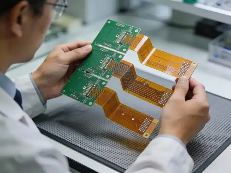
What Is PCB Depaneling and Why Is It So Important?
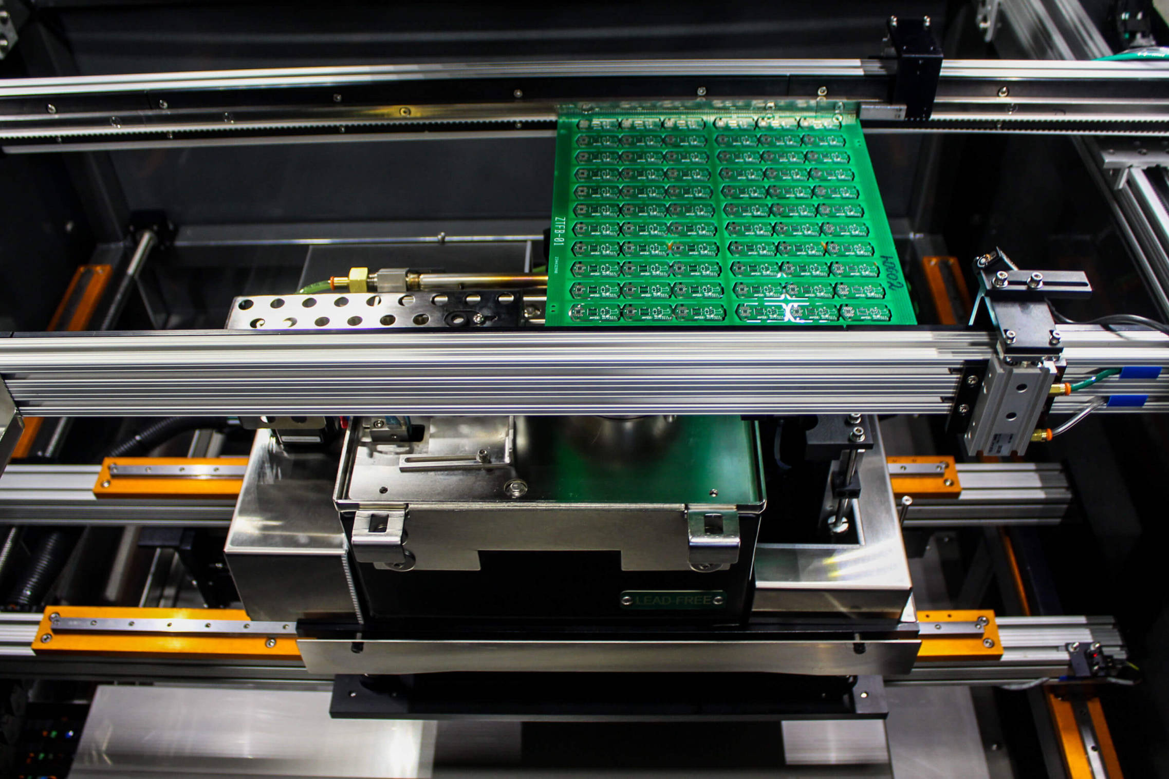
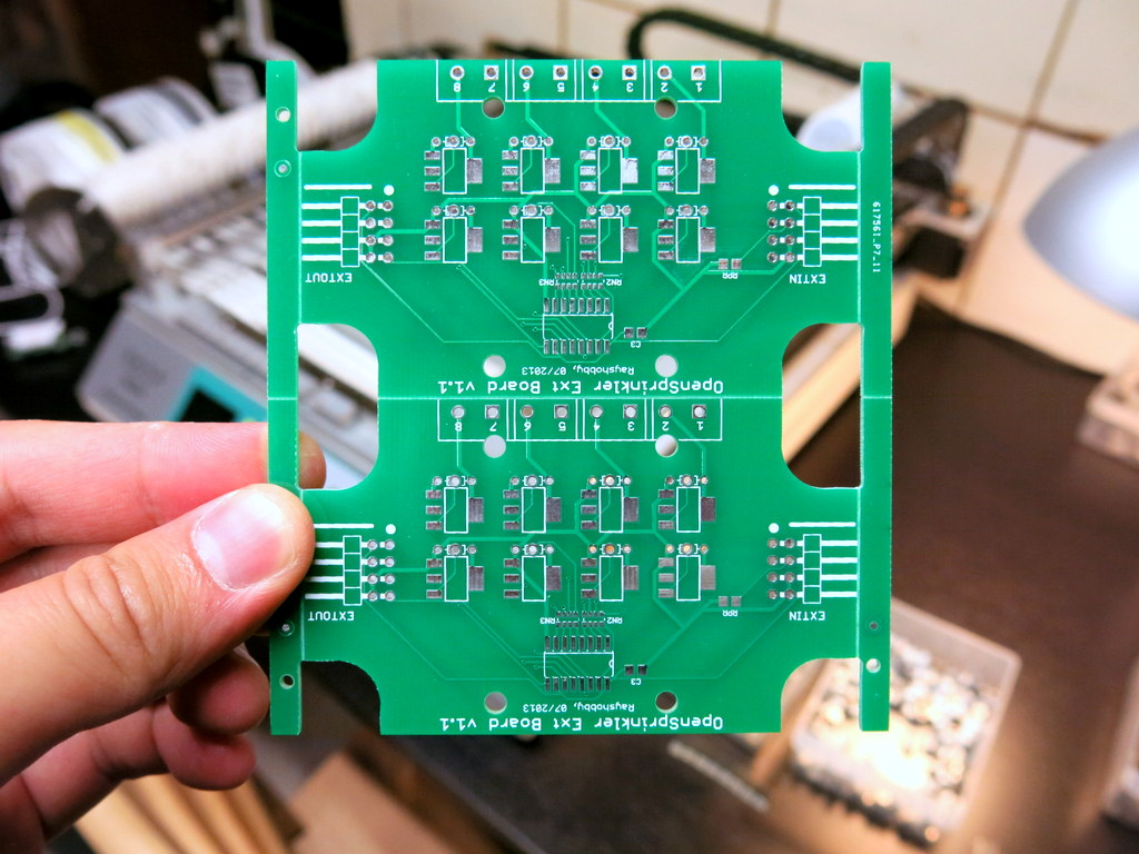
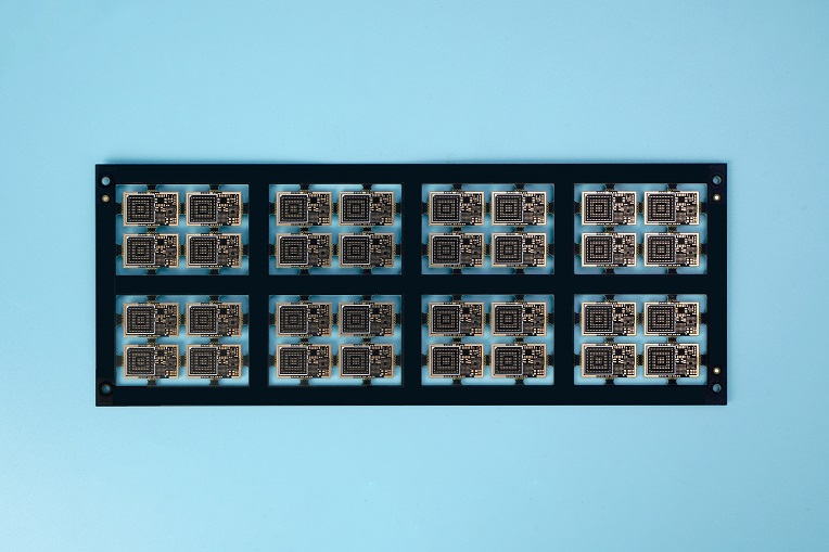
PCB depaneling refers to the crucial process of separating individual circuit boards from a larger manufacturing panel. During fabrication and assembly, multiple PCBs are often produced on a single panel to enhance efficiency and reduce costs. However, the subsequent separation of these boards without causing damage to components, traces, or the board material itself is a delicate and critical step. The chosen depaneling method directly influences the quality of the final product, as well as production speed, cost-effectiveness, and scalability.
Opting for an unsuitable depaneling technique can lead to various problems, including cracked solder joints, compromised board edges, or increased manufacturing expenses. Therefore, a thorough understanding of the distinctions between V-scoring and stamp hole depaneling is essential for engineers and manufacturers aiming to achieve optimal results and deliver high-quality PCBs.
How Does V-Scoring (V-Cut) Depaneling Work?
V-scoring, frequently termed V-cut, involves creating a V-shaped groove on both the top and bottom surfaces of a PCB panel using a specialized cutting tool. This precisely engineered groove strategically weakens the board material along a straight line, allowing for easy separation of individual boards, either manually or with minimal mechanical force. V-scoring is widely adopted in high-volume PCB mass production environments due to its precision and efficiency.
Advantages of PCB V-Scoring
● Precise and Clean Separation: The V-cut method yields smooth board edges with minimal burring, reducing the need for additional post-processing or finishing. This is particularly beneficial for applications where aesthetic appeal or edge quality is paramount.
● Reduced Stress on Components: Since V-scoring requires relatively low force for separation, there is a significantly lower risk of damaging nearby components or delicate solder joints. Research indicates that V-scoring can reduce mechanical stress by as much as 60% compared to some other manual separation techniques.
● Economical for High-Volume Production: V-scoring machines are capable of processing large panels rapidly, making this method highly cost-effective for mass production runs exceeding 10,000 units.
● Compatibility with Automation: The consistent and uniform grooves created by V-scoring facilitate the use of automated depaneling equipment, further accelerating the overall production timeline.
Disadvantages of PCB V-Scoring
● Limited to Straight Lines: V-scoring is only effective for straight-line separations. It cannot be used for PCB designs featuring curved or irregularly shaped board outlines.
● Not Ideal for Thick Boards: This method becomes less efficient for boards thicker than 3.2 mm, as the V-groove may not penetrate sufficiently to allow for easy and clean separation.
● Component Placement Restrictions: Components, especially sensitive ones, cannot be placed too close to the V-cut line (typically requiring a minimum clearance of 0.5 mm) to avoid stress or vibration-induced damage during the cutting process.
V-Cut Design Guidelines
To ensure successful implementation of V-scoring, consider these essential design parameters:
● Groove Depth: The V-cut should ideally penetrate approximately one-third of the board's total thickness from each side. For example, on a 1.6 mm thick board, aim for a 0.5 mm deep groove on both sides, leaving a 0.6 mm web of material in the middle to be broken.
● Minimum Board Spacing: Allow at least 0.3 mm of spacing between individual boards on the panel to accommodate the width of the V-cut tool.
● Component Clearance: Maintain a minimum clearance of 0.5 mm between any components and the V-cut line to prevent damage during the cutting or separation phases.
● Board Thickness Range: V-scoring performs best on boards with thicknesses ranging from 0.6 mm to 3.2 mm. Thicker boards may necessitate alternative depaneling methods.
● Material Compatibility: Verify that your PCB substrate material (e.g., standard FR-4) is suitable for V-scoring, as certain flexible or brittle materials might exhibit unpredictable cracking.
Exploring Stamp Hole Depaneling (Mouse Bites)
Stamp hole depaneling, commonly known as mouse bites, involves drilling a series of small, closely spaced holes along the interconnecting edges where individual PCBs are joined within a larger panel. These perforations effectively weaken the connection, enabling the boards to be manually snapped apart. This method is often preferred for smaller production volumes or for designs where V-scoring is not practical due to complex board shapes.
The Stamp Hole Depaneling Process
The process of stamp hole depaneling is relatively straightforward:
● Design Phase: During the PCB layout stage, small holes (typically ranging from 0.8 mm to 1.2 mm in diameter) are strategically positioned along the designated separation lines. These holes are usually spaced closely together, often between 0.2 mm and 0.5 mm apart.
● Drilling in Fabrication: During fast turn PCB fabrication, these specified holes are drilled into the panel, creating a perforated line that resembles the edge of a postage stamp.
● Separation Post-Assembly: After all components have been assembled onto the panel, the individual boards are separated by snapping them apart, breaking the thin strips of material that remain between the holes.
Stamp Hole Design Specifications
For effective and reliable stamp hole depaneling, adhere to these design guidelines:
● Hole Diameter: Utilize hole diameters between 0.8 mm and 1.2 mm. Holes that are too small may not sufficiently weaken the material, while excessively large holes can consume valuable board space.
● Hole Spacing: Space the holes between 0.2 mm and 0.5 mm apart. This ensures ease of separation without compromising the structural stability of the panel during the assembly process.
● Number of Holes: For a typical 10 mm separation line, generally 5 to 8 holes are sufficient, though this can vary based on the board's material thickness and strength.
● Edge Clearance: Maintain a minimum clearance of 1 mm between any components and the stamp hole line to prevent damage when the boards are snapped apart.
● Material Thickness: Stamp holes are most effective on boards up to 2.0 mm thick. Thicker boards may require considerably more force for separation, increasing the risk of damage.
Advantages of Stamp Hole Depaneling
● Design Flexibility: In contrast to V-scoring, stamp holes can be used for both straight and irregular or curved separation lines, making them highly versatile for unique board geometries.
● Lower Tooling Costs: Stamp holes do not require specialized cutting tools beyond standard drilling equipment, which significantly reduces initial setup costs, especially for smaller production runs (e.g., under 1,000 units).
● Suitability for Small Batches: This method is well-suited for prototyping or low-volume production where the investment in specialized V-scoring machinery is not economically justifiable.
Disadvantages of Stamp Hole Depaneling
● Rough Edges: The snapping action inherent in this process often leaves a rough or jagged edge on the separated boards. This may necessitate additional sanding or finishing steps for aesthetic or functional requirements.
● Increased Board Stress: Breaking boards apart using stamp holes can induce higher mechanical stress on the board and nearby components. Stress levels can be up to 40% greater compared to the V-scoring method.
● Inefficient for High Volumes: Manual separation is a time-consuming process, rendering stamp holes less efficient for large production runs exceeding 5,000 units.
Comparing V-Scoring and Stamp Hole Depaneling: Key Differences
To aid in your depaneling method selection, here’s a comparison of these two techniques based on critical factors:
|
Factor |
V-Scoring (V-Cut) |
Stamp Hole |
|
Separation Line |
Straight lines only |
Straight or irregular lines |
|
Edge Quality |
Smooth, clean edges |
Rough, jagged edges |
|
Stress on Components |
Low (up to 60% less stress) |
Higher (up to 40% more stress) |
|
Production Volume |
Best for high volumes (10,000+ units) |
Best for low volumes (under 1,000 units) |
|
Tooling Cost |
Higher due to specialized equipment |
Lower, uses standard drilling |
|
Board Thickness |
0.6 mm to 3.2 mm |
Up to 2.0 mm |
How to Select the Optimal Depaneling Method
The choice between V-scoring and stamp hole depaneling should align with your project's specific requirements. Consider the following factors to guide your decision:
● Production Volume: For large-scale manufacturing (over 5,000 units), V-scoring's efficiency and automation capabilities make it more cost-effective. For prototypes or smaller runs (under 1,000 units), stamp holes provide a more economical and quicker solution.
● Board Design Complexity: If your PCB layout demands only straight-line separations, V-scoring will deliver superior, clean results. For designs with irregular or curved separation lines, stamp holes are the necessary option.
● Edge Quality Requirements: If smooth, aesthetically pleasing edges are crucial for your application (e.g., for products housed in enclosures or those visible to end-users), V-scoring offers a much better finish. If edge quality is not a primary concern, stamp holes can be adequate.
● Component Density: For boards densely populated with components, especially near the edges, V-scoring minimizes stress and the risk of damage. Stamp holes may pose a higher risk due to the force required for separation.
● Budgetary Constraints: If initial tooling costs are a significant factor, stamp holes require less upfront investment as they utilize standard drilling processes.
● Board Specifications: Verify that your board's thickness falls within the recommended range for the chosen method. Also, confirm that the PCB material (e.g., standard FR-4 versus flexible substrates) is compatible with the selected depaneling technique.
Best Practices for Implementing Your Chosen Depaneling Method
Once a depaneling method has been selected, adhering to these best practices will help ensure a successful outcome:
● Early Collaboration with Manufacturer: Share your design files and discuss your depaneling preferences with your PCB manufacturer during the initial design stages. This proactive communication helps prevent costly revisions and potential manufacturing issues. Specify all tolerances and clearances clearly.
● Prototype Testing: Before committing to full production, fabricate a small batch of prototypes to thoroughly test the chosen depaneling process. For V-scoring, confirm that the groove depth facilitates easy snapping without requiring excessive force. For stamp holes, verify that the hole spacing allows for clean separation without causing damage to the board.
● Optimize Component Placement: Position sensitive components well away from separation lines, adhering strictly to the recommended clearance guidelines (0.5 mm for V-cut, 1 mm for stamp holes).
● Detailed Documentation: Include comprehensive notes within your design files specifying the chosen depaneling method, exact groove depths, or precise hole spacing. This prevents miscommunication during the manufacturing phase.
Common Challenges and How to Mitigate Them
Both V-scoring and stamp hole depaneling can present potential difficulties. Here’s how to effectively address them:
● Board Cracking During Separation: For V-scoring, ensure uniform groove depth across the entire panel. For stamp holes, avoid excessive spacing between holes, as this increases the force needed to snap the boards, raising the risk of cracks.
● Component Damage: Always maintain adequate clearance between components and the separation lines to reduce the impact of vibration or stress.
● Inconsistent Edges: With stamp holes, rough edges are a common outcome. Plan for post-separation finishing steps if a smooth edge is required. For V-scoring, utilize high-quality cutting tools to ensure precise and uniform grooves, preventing uneven edges.
Conclusion: Making the Optimal Choice for Your PCB Project
The decision between V-scoring and stamp hole depaneling ultimately depends on a detailed understanding of your project’s unique requirements. V-scoring excels in high-volume production, offering clean cuts, low mechanical stress, and compatibility with automation, making it ideal for straight-line separations on standard boards. Conversely, stamp hole depaneling provides greater flexibility for irregular board shapes and lower initial costs for small production runs, though it may result in rougher edges and higher mechanical stress.
By carefully evaluating factors such as production volume, board design complexity, desired edge quality, and budget, you can confidently select the most appropriate depaneling method. Utilize the V-cut design guidelines and stamp hole design specifications provided in this guide to optimize your PCB layout for efficient manufacturing. Through meticulous planning and close collaboration with your manufacturing partner, you can achieve precise, damage-free depaneling that perfectly aligns with your project objectives. For further insights into PCB manufacturing processes or assistance with your next project, explore the resources and services offered by AIVON, tailored for engineers and designers seeking dependable solutions.