Introduction
In PCB design, overlooking manufacturability can lead to production delays, increased costs, and frequent rework that frustrates electrical engineers. Critical DFM checks form the backbone of a reliable manufacturability checklist, ensuring designs transition smoothly from layout to fabrication and assembly. These essential PCB design rules address common pitfalls like insufficient clearances and material imbalances that cause PCB assembly errors. By prioritizing these checks early, engineers minimize avoiding PCB rework and achieve higher yields in high-volume runs. Factory experience shows that boards passing these verifications rarely return for fixes, saving time and resources. This article outlines five non-negotiable checks grounded in proven practices.

1. Verify Minimum Trace Width and Spacing Compliance
Trace width and spacing represent foundational elements in any manufacturability checklist. Inadequate dimensions strain etching processes, leading to opens, shorts, or weakened signals during high-speed operations. Electrical engineers must confirm that all signal, power, and ground traces meet or exceed the minimums specified for the chosen fabrication capabilities. Variations in copper thickness across layers demand conservative sizing to prevent under-etching, especially on inner layers where inspection proves challenging. Factory-driven insights reveal that violations here account for a significant portion of initial fab rejects. Adhering to guidelines like those in IPC-2221 ensures reliable current carrying and impedance control without compromising density.
Beyond basic sizing, consider the impact on impedance and crosstalk. Narrow traces amplify resistance losses in power delivery networks, while tight spacing invites bridging during solder reflow. Engineers should run design rule checks (DRC) iteratively, adjusting for stack-up variations. In multilayer boards, outer layer traces tolerate finer features due to better process control, but inner layers require wider margins. This check directly prevents PCB assembly errors like solder shorts, promoting first-pass success.
2. Ensure Adequate Annular Ring on Pads and Vias
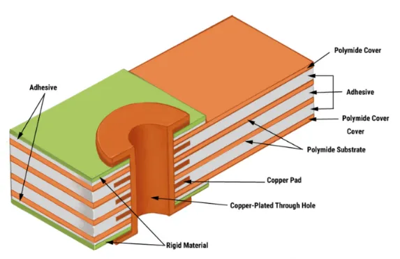
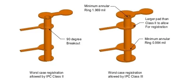
The annular ring, the copper collar surrounding drill holes, stands as a critical DFM check for via and pad reliability. Insufficient ring width risks breakout during drilling or plating, causing intermittent connections or outright opens. Mechanical stresses from assembly exacerbate thin rings, leading to cracks under thermal cycling. Electrical engineers need to specify external and internal ring minimums based on drill size and board class, accounting for drill wander in high-aspect-ratio holes. Factories emphasize breakout-free designs to avoid costly replating or scrapping panels.
Plated through-hole (PTH) vias demand larger rings than surface-mount pads due to plating buildup and tenting challenges. Blind and buried vias introduce additional risks from sequential lamination, requiring even more robust sizing. A thorough review involves simulating drill tolerances and etch factors. This step integrates with essential PCB design rules, safeguarding signal integrity in dense layouts. Neglect here often triggers rework after population, underscoring its priority.
3. Balance Copper Distribution to Prevent Warpage
Uneven copper distribution across layers induces warpage, a pervasive issue in multilayer PCBs that derails assembly. Thermal expansion mismatches during lamination and reflow bow or twist boards, misaligning fiducials and components. Electrical engineers must analyze copper coverage per layer, aiming for balance within 10-15% variance to maintain flatness. Factory processes reveal that heavy copper planes on one side versus light fills on the other amplify bow, especially in thin cores. IPC-A-600 provides acceptability criteria for bow and twist, guiding designs toward compliant outcomes.
Strategies include symmetric stack-ups and strategic plane splits. Fill unetched areas with non-functional copper tied to ground, but avoid isolated islands that etch unevenly. Simulate warpage using finite element analysis for complex boards with high copper asymmetry. This check proves vital for avoiding PCB rework in SMT lines, where warped boards cause pick-and-place failures. Proactive balancing aligns with quality control standards, ensuring dimensional stability post-process.
4. Validate Solder Mask and Silkscreen Specifications
Solder mask defines electrical isolation and solder flow, making its accuracy a key manufacturability checklist item. Overlaps too small on pads lead to solder beading or exposure, while excessive coverage blocks vias or invites delamination. Electrical engineers should enforce minimum clearances around pads, vias, and traces, considering mask registration tolerances. Silkscreen legends require crisp polarity marks and references without overlapping solder areas, preventing reflow smearing. Factories report mask-related defects as common culprits in PCB assembly errors, often necessitating mask revisions.
Liquid photoimageable (LPI) masks demand defined edges to avoid webbing between fine-pitch components. Tent vias properly for QFN and BGA thermal pads, ensuring void-free joints. Review artwork for overlaps on fiducials or test points, which impair inspection. This check supports essential PCB design rules by enhancing assembly yields and long-term reliability. Consistent validation minimizes cosmetic rejects and functional failures.
5. Confirm Fiducials, Panelization, and Tooling Features
Fiducials and panelization features enable precise registration during fabrication and assembly, forming an indispensable DFM check. Absent or poorly placed fiducials confuse optical alignment systems, causing misalignment in depaneling or stencil printing. Electrical engineers must position at least three fiducials asymmetrically, away from board edges and components, with adequate annular rings. V-scoring, tab routing, or perforations require defined margins to prevent cracking during separation. Factories stress tooling holes for handling, typically 3-4mm diameter in corners.
Panel arrays optimize throughput, but over-tight nesting invites warpage or stress concentrations. Include breakaway rails with tooling holes for automated lines, ensuring compatibility with customer equipment. Simulate depaneling stresses to validate routing paths. This comprehensive review prevents avoiding PCB rework by streamlining the entire production flow. Integration with upstream checks yields panels ready for high-speed assembly.
Building Your Comprehensive Manufacturability Checklist
Integrating these five critical DFM checks creates a robust framework for electrical engineers. Start with DRC automation, followed by manual layer-by-layer audits. Collaborate with fabrication partners for capability matrices, tailoring rules to specific processes. Track historical yields to refine checklists iteratively. Common oversights like ignoring aspect ratios or thermal reliefs compound errors, but diligence here slashes defect rates.
-
Trace Width/Spacing — Key Focus Areas: Minimum dimensions per layer; Potential Risks if Skipped: Opens, shorts, impedance issues.
-
Annular Ring — Key Focus Areas: Drill size tolerances; Potential Risks if Skipped: Breakouts, plating voids.
-
Copper Balance — Key Focus Areas: Coverage uniformity; Potential Risks if Skipped: Warpage, bow/twist.
-
Solder Mask/Silkscreen — Key Focus Areas: Clearances, overlaps; Potential Risks if Skipped: Solder defects, legend smearing.
-
Fiducials/Panelization — Key Focus Areas: Placement, margins; Potential Risks if Skipped: Misalignment, depaneling damage.
This list serves as a quick reference for design reviews, promoting consistency.
Conclusion
Skipping these critical DFM checks invites PCB assembly errors and rework cycles that erode project timelines. Electrical engineers benefit from embedding essential PCB design rules into workflows, leveraging standard-aligned practices for superior outcomes. Balanced designs not only fabricate reliably but also assemble with minimal intervention. Prioritize verification at each stage to unlock efficient production. Ultimately, a proactive manufacturability checklist transforms potential pitfalls into strengths.
FAQs
Q1: What are the most critical DFM checks for PCB manufacturing?
A1: Critical DFM checks include trace width compliance, annular ring integrity, copper balance, solder mask validation, and fiducial placement. These essential PCB design rules prevent fabrication defects and ensure smooth assembly. Factory insights confirm they reduce rejects by addressing root causes like etching errors and warpage early.
Q2: How can engineers avoid common PCB assembly errors?
A2: Engineers avoid PCB assembly errors by verifying component spacing, thermal reliefs, and panelization in their manufacturability checklist. Adequate fiducials and balanced copper distribution minimize misalignment and warpage during reflow. Consistent DRC runs aligned with fabrication capabilities catch issues pre-production.
Q3: Why is copper balance a key part of avoiding PCB rework?
A3: Copper balance prevents warpage by equalizing stresses across layers, a vital manufacturability checklist item. Uneven distribution causes bow during lamination or reflow, leading to pick-and-place failures. Engineers achieve it through symmetric fills and stack-up symmetry, aligning with acceptability standards.
Q4: What role do fiducials play in essential PCB design rules?
A4: Fiducials enable precise machine vision for stencil printing and depaneling, integral to essential PCB design rules. Place them asymmetrically with clear annular rings to support automated processes. This check avoids alignment errors, streamlining assembly and reducing rework.
References
IPC-2221B — Generic Standard on Printed Board Design. IPC, 2012
IPC-6012E — Qualification and Performance Specification for Rigid Printed Boards. IPC, 2017
IPC-A-600K — Acceptability of Printed Boards. IPC, 2020