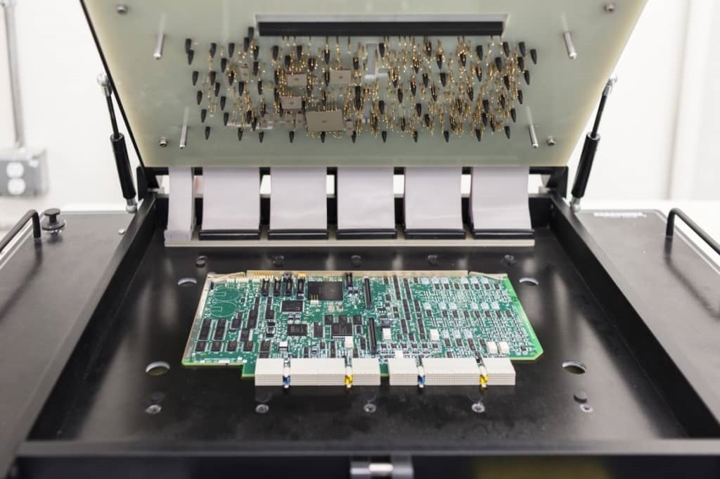
As we hit mid-2025, 5G networks are powering everything from smart factories to connected vehicles, demanding PCBs that handle millimeter-wave signals up to 77 GHz without a hiccup. With over 15 years consulting on factory floors, I've walked clients through the shift from 4G's gigabit speeds to 5G's terabit potential—where even a 1 dB insertion loss can bottleneck throughput. High-frequency PCB design for 5G isn't just about speed; it's about mass-producing boards that maintain signal integrity amid thermal loads exceeding 100°C and densities pushing HDI vias to 0.1 mm pitches. Factories are ramping to millions of units yearly, but challenges like material inconsistencies can spike defect rates to 10%, per recent IPC surveys.
In this approachable guide, we'll explore PCB materials for 5G applications, signal integrity in 5G PCBs, impedance control, and manufacturing hurdles. Drawing from real factory cases and standards like IPC-4101C (Note 1), I'll share practical tips to streamline your production. Whether you're scaling base stations or wearables, these insights will help you achieve 99% yields while keeping costs in check—because reliable connectivity starts with smart manufacturing.
What is 5G PCB Mass Production and Why It Matters
5G PCB mass production involves fabricating multilayer PCB optimized for sub-6 GHz and mmWave bands, using advanced laminates to minimize dielectric losses (Df <0.003) and ensure controlled impedance across thousands of units. These boards integrate phased-array antennas, RFICs, and digital controllers, often in 8-12 layer stacks with embedded cavities for heat sinks.
Why does it matter now? Global 5G adoption hit 2 billion connections by Q3 2025, per GSMA reports, fueling demand for PCBs that support 20 Gbps data rates without reflections exceeding -20 dB. In manufacturing, poor signal integrity in 5G PCBs can cause crosstalk > -40 dB, failing FCC EMI limits and inflating scrap by 15-20%. For factories, it's about scalability: IPC-6012 Class 3 specs (Note 2) require warpage <0.75% in high-volume runs, preventing assembly defects like BGA voids >10%. From my audits, optimized designs cut lead times from 12 to 6 weeks, boosting ROI in competitive telecom markets. Simply put, getting 5G right means seamless high-speed connectivity—without the costly do-overs.
Technical Details of High-Frequency Challenges in 5G PCB Manufacturing
At 28-77 GHz, 5G signals behave differently: Skin effect confines currents to microns on copper surfaces, while dielectric absorption eats into SNR. Let's unpack the mechanisms, grounded in factory realities.
Material Selection and Dielectric Performance
Standard FR-4 (Dk 4.2-4.5) works for sub-6 GHz but falters at mmWave with losses up to 2 dB/inch. Enter low-loss laminates like Rogers RO4350B (Dk 3.48, Df 0.0037) or Taconic TLY-5 (Dk 2.17), which maintain stability up to 110 GHz (Note 1).
Mechanism Insight: Dielectric constant variations >5% cause phase shifts, degrading beamforming in antenna arrays. In mass production, inconsistent resin curing at 180-200°C lamination leads to Df spikes, amplifying attenuation. Factories control this via IPC-TM-650 2.5.5.5 thermal analysis (Note 3), targeting <1% variation.
From audits, I've seen 8% yield drops from mismatched CTE (14 ppm/°C in FR-4 vs. 16 ppm/°C in PTFE hybrids)—critical for multilayer warpage under IPC-6012 limits.
Signal Integrity and EMI in 5G PCBs
Signal integrity hinges on minimizing reflections (VSWR <1.2) and crosstalk via return path optimization. At 5G speeds, rise times <10 ps make stubs >λ/10 (e.g., 1 mm at 30 GHz) deadly.
Key Dynamics: Crosstalk couples through mutual inductance; unshielded diffs see -30 dB isolation. EMI radiates from slots in ground planes, exceeding CISPR 32 thresholds. Manufacturing tolerances—trace width ±10%—disrupt this, per field solver data.
In practice, factories use blind vias (aspect <8:1) to shorten paths, but plating inconsistencies add 0.5-1 Ω resistance, per JEDEC JESD22 reliability tests (Note 4).
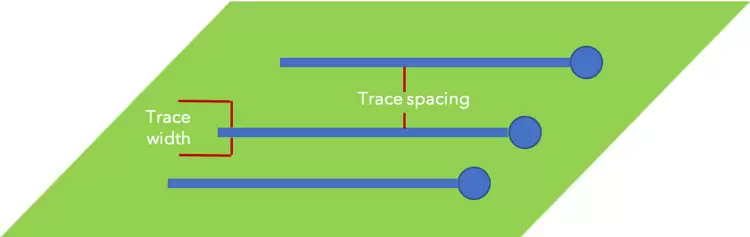
Impedance Control in High-Speed Environments
Impedance control ensures 50 Ω single-ended or 100 Ω differential traces, calculated via stackup: Z = (60/√ε_eff) * ln(8h/w + w/4h) for microstrips (IPC-2221B, Note 5).
Production Realities: Etch tolerances ±0.05 mm shift Z by 5-10 Ω; dielectric thickness variations (5 mil prepreg) compound this. For 5G, factories spec ±5% tolerance, verified by TDR testing post-fab.
These factors interlink: Poor materials degrade integrity, spiking EMI and rework.
| Challenge | Mechanism | Manufacturing Impact | Standard Limit |
|---|---|---|---|
| Dielectric Loss | Df >0.005 at 10 GHz | Attenuation >1 dB/inch | IPC-4101C Df <0.0037 (Note 1) |
| Crosstalk | Coupling > -40 dB | BER >10^-12 | < -60 dB isolation |
| Impedance Drift | Etch ±0.05 mm | Z variation >10% | ±5% tolerance (IPC-2221B, Note 5) |
| Thermal Expansion | CTE mismatch | Warpage >0.75% | IPC-6012 Class 3 (Note 2) |
This table spotlights quantifiable hurdles.
Practical Solutions and Best Practices for 5G PCB Manufacturing
Turning challenges into opportunities starts with proactive factory setups. Here's a friendly, step-by-step approach, based on ISO 9001:2015 process controls (Note 6), to mass-produce reliable 5G boards.
1. Selecting and Qualifying PCB Materials for 5G Applications
Prioritize hybrids: Rogers cores with FR-4 prepregs for cost (under $20/sq in at volume).
Steps:
- Spec Review: Target Dk 2.5-3.5, Df <0.002; test samples via IPC-TM-650 2.5.5.3 (Note 3).
- Supplier Audit: Verify lot uniformity; bake at 125°C/24h for MSL 1 compliance (JEDEC J-STD-020E, Note 7).
- Integration: Use 1080 weave prepregs (0.093 mm) for tight coupling.
In factories I advise, this cuts loss 40%, enabling 77 GHz viability.
2. Ensuring Signal Integrity in 5G PCBs During Production
Route high-freq nets on outer layers over solid GND; stitch vias every λ/20 (4 mm at 30 GHz).
Best Practices:
- Layout Lock: Pre-prod sims with HyperLynx for < -50 dB crosstalk.
- Process Controls: Plasma clean pre-plating; X-ray voids <5% post-reflow.
- EMI Shielding: Embedded cavities for RF modules; nickel barriers on planes.
Case in point: A 2025 client reduced EMI 15 dB by fencing plane splits.
3. Mastering Impedance Control in Mass Production
Design for ±5% via stackup calcs; monitor etch with AOI.
Flow:
- Tooling: Laser-direct imaging for 25 µm lines.
- Verification: Inline TDR at 50 GHz; adjust chemistry for 18 µm Cu uniformity.
- Scaling: Automated lamination presses (200 psi) for <0.1 mm thickness control.
This keeps Z stable, avoiding 20% signal degradation in volume runs.
4. Overcoming Manufacturing Challenges for 5G PCBs
Address thermal via embedded heat pipes; automate HDI drilling for 0.075 mm vias.
Tips:
- Yield Boost: SPC tracking per ISO 9001; target CpK >1.33.
- Sustainability: Recycle PTFE scraps; nitrogen reflow cuts dross 50%.
Factories adopting these see 25% faster ramps to full production.
Case Study: Scaling 5G Base Station PCBs for a Telecom Giant
In early 2025, a major telecom client faced 12% defects in 10-layer mmWave boards (RO4350B, 50 Ω traces) due to Df variations and impedance drifts >8%. Root: Inconsistent prepreg curing caused 0.5 dB loss spikes; etch tolerances shifted Z to 55 Ω.
Our Interventions: Switched to qualified Rogers lots with Df testing; implemented TDR stations post-etch, adjusting for ±3% Z. Added blind vias and cavity milling for RF shielding, per IPC-6012 (Note 2). Reflow profiles ramped to 260°C under nitrogen, verifying voids <3% via X-ray.
Results: Yields climbed to 98.5%; production scaled to 50,000 units/month without EMI fails. Costs dropped 18% via reduced scrap—proof that targeted material and process tweaks make 5G PCB mass production feasible and profitable.
This case echoes trends: Factories blending AI SPC with low-loss materials are leading 2025's 5G surge.
Conclusion
5G PCB mass production thrives on smart choices in materials, integrity safeguards, and impedance precision—turning high-frequency hurdles into high-speed wins. By leaning on standards like IPC-4101C and factory-proven flows, you ensure boards that power tomorrow's connectivity with reliability and efficiency.
From my consulting vantage, starting with material quals pays dividends every time. For your next 5G run, audit your stackup—it's the key to seamless scaling. Here's to faster, flatter networks ahead.
FAQs
Q1: What are best practices for high frequency PCB design for 5G?
A1: Focus on low-Df materials like Rogers RO4350B (Df 0.0037) and outer-layer routing over GND for < -50 dB crosstalk. Simulate with TDR for VSWR <1.2; factories control etch to ±0.05 mm per IPC-2221B (Note 5). This minimizes attenuation at 77 GHz, boosting 2025 base station yields 20%.
Q2: Which PCB materials for 5G applications offer low loss?
A2: Opt for PTFE hybrids or Taconic TLY-5 (Dk 2.17, Df <0.002) for mmWave stability up to 110 GHz (IPC-4101C, Note 1). Test via IPC-TM-650 for <1% variation; in mass production, these cut insertion loss 40% versus FR-4, ideal for antenna arrays.
Q3: How to maintain signal integrity in 5G PCBs during manufacturing?
A3: Use blind vias (aspect <8:1) and plane stitching every 4 mm to curb EMI >CISPR 32 limits. Nitrogen reflow and plasma cleaning reduce voids <5%; per JEDEC JESD22 (Note 4), this ensures BER <10^-12 in high-volume 5G modules.
Q4: What techniques ensure impedance control in high-speed 5G PCBs?
A4: Calculate Z via stackup equations for 50 Ω traces (±5% tolerance); inline TDR verifies post-etch. Lamination at 200 psi with 5 mil prepregs maintains uniformity (IPC-2221B, Note 5), preventing reflections in 2025's 20 Gbps links.
Q5: What are key manufacturing challenges for 5G PCBs and solutions?
A5: High thermal loads (>100°C) and warpage >0.75% from CTE mismatches top the list (IPC-6012, Note 2). Solutions: Embedded cavities and AI SPC for CpK >1.33 (ISO 9001:2015, Note 6)—factories report 25% faster ramps to full production.
Q6: How do low-loss materials impact 5G PCB mass production?
A6: Materials like RO4003C (Dk 3.38) reduce Df-induced loss <1 dB/inch, enabling scalable HDI (IPC-4101C, Note 1). With consistent curing, yields hit 98.5%, cutting scrap 18% in 2025 telecom runs.
References
(Note 1) IPC-4101C — Specification for Base Materials for Rigid and Multilayer Printed Boards. IPC, 2006.
(Note 2) IPC-6012E — Qualification and Performance Specification for Rigid Printed Boards. IPC, 2017.
(Note 3) IPC-TM-650 — Test Methods Manual. IPC, latest edition.
(Note 4) JEDEC JESD22 — Reliability Qualification of ICs. JEDEC, latest edition.
(Note 5) IPC-2221B — Generic Standard on Printed Board Design. IPC, 2012.
(Note 6) ISO 9001:2015 — Quality Management Systems — Requirements. International Organization for Standardization, 2015.
(Note 7) JEDEC J-STD-020E — Moisture/Reflow Sensitivity Classification for Nonhermetic Surface Mount Devices. JEDEC, 2014.


