Introduction
Printed circuit boards form the backbone of most electronic projects, and for hobbyists, mastering basic components like vias opens up reliable designs. Understanding PCB vias starts with recognizing them as small plated holes that connect copper layers electrically. In simple setups, such as LED drivers or sensor boards, unfilled vias can lead to soldering challenges or mechanical weaknesses. This is where via filling comes into play, a technique that seals these holes with specialized materials. What is via filling? It involves depositing conductive or non-conductive substances inside the via to enhance performance, prevent contamination, and ensure a flat surface for components. For electronic hobbyists tackling simple PCB projects via filling, this guide breaks down the essentials in clear steps.
Via filling matters because hobbyist prototypes often face hand-assembly stresses that empty vias cannot withstand. Without proper filling, solder can wick into vias during soldering, reducing joint strength and causing intermittent connections. Filled vias also improve heat dissipation in power circuits, a common need in battery-powered gadgets. Hobbyists benefit from these basics without needing advanced factory processes. This article explores definitions, types, techniques, and practical applications tailored to home workshops.
What Are PCB Vias and Why Consider Via Filling?
PCB vias serve as vertical interconnects in multilayer boards, allowing signals or power to travel between layers. In hobbyist designs, through-hole vias dominate due to their simplicity in etching and plating during fabrication. These vias consist of a drilled hole lined with copper plating for conductivity, but the open barrel leaves room for issues like flux residue buildup or plating cracks over time. Understanding PCB vias means appreciating their role in routing traces efficiently while minimizing board space.
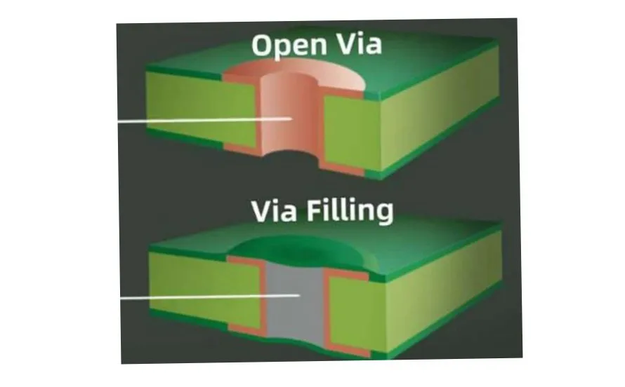
What is via filling exactly? It is the process of completely or partially filling the via's interior with materials like epoxy resin or conductive pastes after plating. This step addresses reliability concerns outlined in industry standards such as IPC-6012E, which specifies performance for rigid printed boards. Filling eliminates air pockets that could trap moisture, leading to failures in humid environments common for hobbyist storage. For beginners, via filling transforms a basic via into a robust feature suitable for repeated handling.
Hobbyists encounter via issues in prototypes where boards flex during testing or assembly. Empty vias act as stress concentrators, potentially cracking under thermal cycles from soldering irons. Filling distributes stress evenly, aligning with acceptability criteria in IPC-A-600K. Moreover, it creates a planar surface, easing the placement of surface-mount parts in dense layouts. In essence, via filling elevates simple designs to production-like quality without complexity.
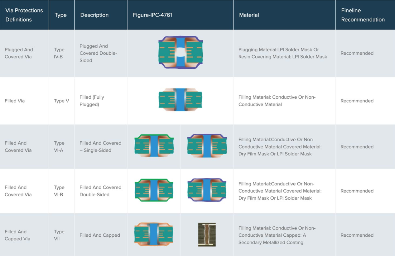
Types of Via Filling for Hobbyists
Types of via filling for hobbyists focus on accessible materials that require minimal equipment. Non-conductive epoxy filling tops the list for its ease and low cost, using clear resins cured with heat or UV light. This type insulates the via electrically while providing mechanical support, ideal for signal layers where capacitance changes must be avoided. Hobbyists apply it via syringe after cleaning the via, ensuring no voids form during curing.
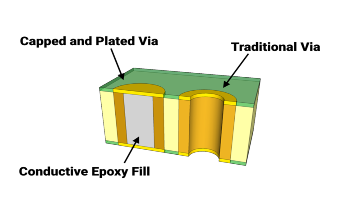
Conductive via filling suits power or ground planes needing thermal relief. Silver or copper-filled epoxies conduct heat and electricity, reducing thermal resistance compared to plated walls alone. These pastes sinter at moderate temperatures, compatible with oven curing in home setups. For hobbyists, the choice depends on project needs, like heat sinking in motor drivers.
A third option, solder filling, involves melting low-melt solder into vias during reflow, though it risks bridging nearby pads. This method works for prototypes but demands precise control to avoid excess flow. Each type aligns with J-STD-001 requirements for soldered connections, emphasizing clean fills without defects. Hobbyists select based on board thickness and layer count, starting simple.
Basic Via Filling Techniques for Home Workshops
Basic via filling techniques begin with preparation to ensure adhesion and reliability. First, clean the board post-fabrication using isopropyl alcohol to remove residues from drilling or plating. Inspect vias under magnification for plating uniformity, rejecting any with voids. Mask surrounding areas with tape to prevent spills during filling.
For non-conductive filling, dispense epoxy into vias using a fine-tip syringe, tapping the board gently to release air bubbles. Cure in an oven at manufacturer-specified temperatures, typically 100 to 150 degrees Celsius for 1 to 2 hours. Post-cure, plane the surface with fine sandpaper if excess protrudes, followed by a solvent wipe. This technique suits hobbyists building audio amplifiers where vias carry audio signals without interference.
Conductive paste application follows similarly but requires vacuum assistance for dense packing in deeper vias. Apply paste, then use a vacuum chamber or desiccator to draw out air, maximizing fill density. Cure under controlled heat to activate conductivity, testing continuity afterward with a multimeter. These steps mirror factory processes scaled for desktops.
Solder filling involves fluxing vias, then heating with a hot air station while feeding solder wire. Control temperature to 250 degrees Celsius to avoid delamination. Clean flux residues promptly to prevent corrosion. All techniques prioritize safety, using ventilation for fumes.
Simple PCB Projects Benefiting from Via Filling
Simple PCB projects via filling shine in applications demanding durability on a budget. Consider a basic LED matrix driver board with multiple power layers. Unfilled vias in ground planes wick solder during hand assembly, starving LED joints. Filling with conductive paste ensures robust thermal paths, keeping LEDs cool during matrix scans.
Another project is a sensor hub for IoT prototypes, routing analog signals across layers. Non-conductive filling prevents crosstalk while sealing vias against dust in workshop environments. Hobbyists etch these at home or order from basic services, filling post-arrival for customization. The result is a stable board handling temperature fluctuations.
Power distribution boards for robotics motors exemplify thermal needs. Conductive-filled vias act as heat pipes, dissipating joule heating from high currents. In a simple rover chassis controller, this prevents hotspots that warp unfilled boards. Testing shows filled versions withstand vibration better, crucial for mobile projects.
Even single-layer adapters benefit, where stacked vias connect breakout headers. Epoxy filling adds strength against probe insertions. These projects demonstrate via filling's versatility for hobbyists scaling from breadboards.
Best Practices and Common Pitfalls to Avoid
Adopt best practices by matching fill type to via size and board material. For vias under 0.3 mm diameter, prefer low-viscosity epoxies to avoid clogging. Always document fill parameters for repeatability in iterative designs. Test filled boards with continuity checks and thermal imaging if available.
Avoid overfilling, which causes doming and solder mask adhesion issues. Underfilling leaves weak spots prone to cracking per IPC standards. Cure fully before handling to prevent cracks from thermal shock. Store materials in cool, dry places to maintain viscosity.
In assembly, reflow after filling only if the material tolerates it, checking datasheets. For hand soldering, pre-fill critical vias to streamline workflow. These habits build confidence in via-filled prototypes.
Conclusion
Mastering via filling equips hobbyists with tools for reliable PCBs beyond basic traces. From understanding PCB vias to applying basic via filling techniques, each step enhances project outcomes. Types of via filling for hobbyists offer choices from epoxy to conductive pastes, fitting simple PCB projects via filling needs. Prioritize cleanliness, proper curing, and standard compliance for success. Experiment on scrap boards first, gradually integrating into designs. This foundation supports advancing to complex builds with confidence.
FAQs
Q1: What is via filling in PCBs?
A1: Via filling is the process of injecting conductive or non-conductive materials into plated via holes to improve mechanical strength, thermal performance, and surface planarity. For hobbyists, it prevents solder wicking during hand assembly and seals against contaminants. This technique aligns with IPC-6012E specifications for board reliability, making prototypes more durable without advanced tools. Beginners start with epoxy for quick results.
Q2: What are the main types of via filling for hobbyists?
A2: Types of via filling for hobbyists include non-conductive epoxy for insulation and planarity, conductive pastes for heat dissipation, and solder for simple thermal vias. Epoxy suits signal layers in sensor boards, while conductive fills aid power circuits. Choose based on project needs, ensuring compatibility with curing ovens. These options keep costs low for home workshops.
Q3: What are basic via filling techniques for beginners?
A3: Basic via filling techniques involve cleaning vias, dispensing material with a syringe, removing bubbles by tapping or vacuum, and curing in an oven. Inspect for voids post-cure and plane excess for flatness. Use magnification for precision on small boards. This method supports understanding PCB vias in prototypes without factory equipment.
Q4: When should hobbyists use via filling in simple projects?
A4: Use via filling in simple PCB projects via filling scenarios like power boards or multilayer sensors where thermal stress or solder issues arise. It strengthens vias against flexing and improves heat flow in LED drivers. Skip for low-stress signal routing to save time. Always test filled boards for continuity.
References
IPC-6012E — Qualification and Performance Specification for Rigid Printed Boards. IPC, 2017
IPC-A-600K — Acceptability of Printed Boards. IPC, 2020
J-STD-001H — Requirements for Soldered Electrical and Electronic Assemblies. IPC, 2018


