Introduction
In modern high-speed electronics, printed circuit boards (PCBs) must support data rates exceeding several gigabits per second, making signal integrity a critical design factor. PCB via stubs emerge as a common challenge in multilayer boards, where through-hole vias extend beyond the active signal layers, creating unwanted extensions that degrade performance. These stubs lead to signal reflections that distort waveforms and reduce eye opening in high-speed links. Controlled depth drilling, often referred to as backdrilling, offers a practical solution by precisely removing these stubs to enhance signal integrity improvement. This article explores PCB via stubs, their causes of signal reflection, backdrilling benefits, and key PCB design considerations for electrical engineers optimizing complex designs. By understanding these elements, designers can achieve reliable performance without excessive costs.
Understanding PCB Via Stubs
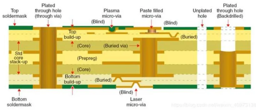
A PCB via stub refers to the unused portion of a plated through-hole (PTH) via that extends past the last inner layer connected to the signal trace. In multilayer PCBs, PTH vias traverse the entire board thickness to connect surface layers, but signals often only interact with inner layers, leaving the excess barrel length as a stub. This stub acts as an unintended transmission line segment terminated in an open circuit, fundamentally altering impedance characteristics. Engineers encounter via stubs frequently in designs with more than eight layers, where routing density demands through vias for efficiency. Without mitigation, these structures compromise high-frequency signals by introducing discontinuities. Proper identification during stackup planning is essential for PCB design considerations.
The Impact of Via Stubs on Signal Integrity
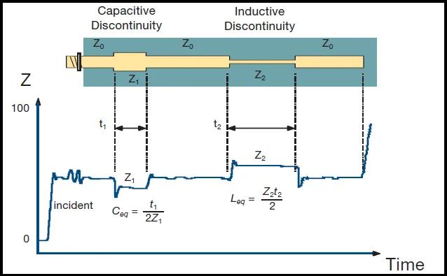
Signal reflection from PCB via stubs arises due to impedance mismatch at the stub's open end, where the signal encounters a high-impedance boundary after propagating through the via. This reflection travels back toward the source, interfering with the original waveform and causing inter-symbol interference (ISI) in serial links. At frequencies above 1 GHz, stub lengths equivalent to a fraction of the signal rise time become resonant, amplifying distortions and reducing insertion loss margins. Electrical engineers observe this in time-domain reflectometry (TDR) traces, where via stubs produce characteristic impedance dips followed by spikes. In backplane applications, unaddressed via stubs can limit channel lengths and data rates, necessitating signal integrity improvement strategies early in the design cycle. Quantifying stub effects through simulation helps prioritize mitigation for critical nets.
Technical Principles Behind Signal Reflection
Transmission line theory governs signal behavior in PCBs, treating vias as coaxial or stripline structures with characteristic impedance around 50 ohms. When a signal reaches the stub end, partial reflection occurs according to the reflection coefficient formula, Γ = (Z_L - Z_0)/(Z_L + Z_0), where Z_L approaches infinity for an open stub. The reflected wave superimposes on incoming signals, creating ringing and overshoot that eye diagrams reveal as closure. Stub length determines the primary resonance frequency, roughly f = c / (4 * L_stub), where c is the speed of light adjusted for dielectric constant. In practice, stubs shorter than one-tenth the rise time equivalent electrical length minimize impact, but multilayer stackups often exceed this threshold. IPC-6012 provides qualification criteria for vias, indirectly supporting stub management through plating and hole quality requirements.
Controlled Depth Drilling: The Backdrilling Process
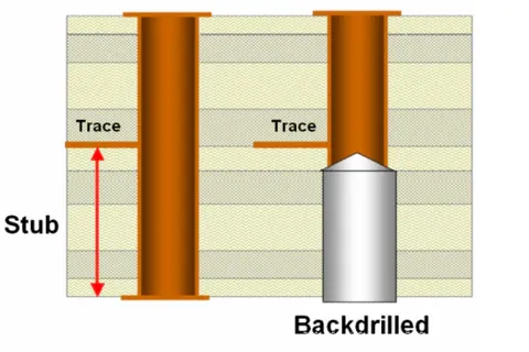
Controlled depth drilling, or backdrilling, involves using a larger-diameter drill bit from the opposite board side to remove the via stub while preserving the connected portion. The process starts after PTH plating, targeting a depth that stops short of the innermost landing pad by a controlled margin. Manufacturers employ peck drilling techniques to evacuate debris and maintain precision, ensuring the backdrill does not encroach on active layers. Aspect ratios for backdrills typically mirror initial via drills, but tolerances tighten to ±0.10 mm for depth accuracy in high-layer-count boards. This method contrasts with blind or buried vias, offering a post-design fix for cost-sensitive prototypes. Successful backdrilling demands clear fabrication notes specifying target depths and overshoot allowances.
Backdrilling Benefits for Signal Integrity Improvement
Backdrilling delivers substantial backdrilling benefits by shortening effective via length, reducing return loss by up to 20 dB in simulations for multi-Gbps signals. Eliminating stubs minimizes reflections, widening eye openings and extending reach in SerDes channels without active equalization. Signal integrity improvement extends to lower crosstalk, as stub resonances no longer couple noise to adjacent nets. In production, backdrilled boards exhibit consistent performance across batches, aligning with IPC-A-600 acceptability criteria for hole walls and plating integrity post-drilling. Designers appreciate the technique's scalability for high-volume runs, where it balances cost against blind via expenses. Overall, it enables denser routing while upholding electromagnetic compatibility.
PCB Design Considerations for Via Stubs and Backdrilling
Effective PCB design considerations begin with stackup optimization to minimize stub lengths, prioritizing signals on outer layers for critical high-speed nets. During routing, allocate backdrill sites by marking opposite-side clearances and specifying stub targets in drill files. Backdrill bit size must exceed the PTH by at least 0.15 mm to avoid residue, while maintaining sufficient annular ring on landing pads. Simulate TDR and S-parameters to validate stub removal efficacy before fabrication. Tolerances for depth control depend on board thickness and layer count, requiring coordination with capabilities documented in fabrication guidelines. Integrating these practices prevents yield issues from overdrilling or incomplete stub removal.
- Stub Target Length — Less than 1/10 rise time equivalent
- Backdrill Oversize — 0.10-0.25 mm larger than PTH
- Depth Tolerance — Typically ±0.10 mm
- Annular Ring Clearance — Minimum 0.15 mm from active pad
- Layer Pairing — Pair signals for symmetric backdrills
Best Practices in Implementing Controlled Depth Drilling
Start with thorough DFM analysis, defining backdrill depths per via in a dedicated table within Gerber notes. Use simulation tools to predict post-backdrill impedance profiles, ensuring continuity with trace Z0. Verify process capability through test coupons measuring depth variation and stub remnants via cross-sectioning. IPC-6012 acceptance criteria apply to backdrilled features, mandating uniform plating removal and smooth walls. For asymmetric stackups, sequence backdrills to avoid warpage from uneven material removal. Post-fabrication, inspect with automated optical systems for overshoot detection, confirming signal integrity improvement.
Troubleshooting Common Backdrilling Challenges
Engineers often face incomplete stub removal due to drill wander in thick boards, addressed by reducing peck depth and feed rates. Residue on backdrill walls can degrade plating adhesion, mitigated by plasma cleaning pre-plating. Depth overshoot risks damaging inner traces, preventable through precise entry-exit targeting and pilot holes. Warpage from unbalanced drilling pairs calls for sequential processing on both sides. Electrical testing via VNA confirms reflection coefficients below -20 dB. Documenting lessons refines future PCB design considerations.
Conclusion
PCB via stubs pose significant risks to signal integrity through reflections in high-speed designs, but controlled depth drilling provides a reliable countermeasure. By grasping the principles of signal reflection and implementing backdrilling benefits, engineers can enhance performance without redesigning stackups. Key PCB design considerations, from stub length calculations to fabrication tolerances, ensure successful outcomes. Adhering to standards like IPC-6012 and IPC-A-600 upholds quality. Ultimately, proactive via management unlocks higher data rates and reliability in demanding applications.
FAQs
Q1: What are PCB via stubs and how do they cause signal reflection?
A1: PCB via stubs are the excess lengths of through-hole vias beyond active layers in multilayer boards. They create an open-circuit termination, generating reflections due to impedance discontinuity. These reflections interfere with high-speed signals, causing ISI and eye closure. Mitigating stubs via backdrilling is essential for signal integrity improvement in designs above 5 Gbps.
Q2: What are the main backdrilling benefits for high-speed PCBs?
A2: Backdrilling removes via stubs, reducing return loss and extending channel lengths. It improves signal integrity by minimizing reflections and crosstalk without needing blind vias. This technique supports denser routing and cost-effective fabrication for production volumes. Electrical engineers value its compatibility with standard processes per IPC guidelines.
Q3: How do PCB design considerations influence via stub management?
A3: Designers must calculate stub lengths against rise times and specify backdrill depths accurately. Stackup symmetry and annular ring clearances prevent overshoot issues. Simulation validates impedance continuity post-backdrilling. These considerations ensure reliable signal performance in complex multilayer boards.
Q4: When should engineers opt for controlled depth drilling over other via types?
A4: Choose backdrilling for cost-sensitive high-layer-count boards where PTH vias are unavoidable. It excels in prototypes and volumes needing signal integrity improvement without HDI premiums. Avoid for ultra-fine pitch or when blind vias suffice for low stub needs. Fabrication feedback guides the decision.
References
IPC-6012E — Qualification and Performance Specification for Rigid Printed Boards. IPC, 2017
IPC-A-600K — Acceptability of Printed Boards. IPC, 2020
IPC-2221B — Generic Standard on Printed Board Design. IPC, 2012