Introduction
High-density interconnect (HDI) printed circuit boards (PCBs) are integral to modern electronics, enabling compact designs with intricate layouts. Among the critical features in these boards, plated edges play a significant role in enhancing connectivity and structural integrity. Edge plating in PCBs involves applying a conductive layer along the board's perimeter, often to improve grounding, shielding, or mechanical strength. However, achieving reliable plated edges in high-density designs requires meticulous attention to design for manufacturing (DFM) principles. This guide explores the essentials of DFM for edge plating, focusing on controlled depth plating and impedance control for plated edges. Aimed at electrical engineers, this article provides actionable insights to optimize designs, reduce manufacturing defects, and ensure performance in HDI applications. Understanding these concepts is vital for tackling the challenges of complex PCB layouts.
What Are Plated Edges and Why Do They Matter in HDI PCBs?
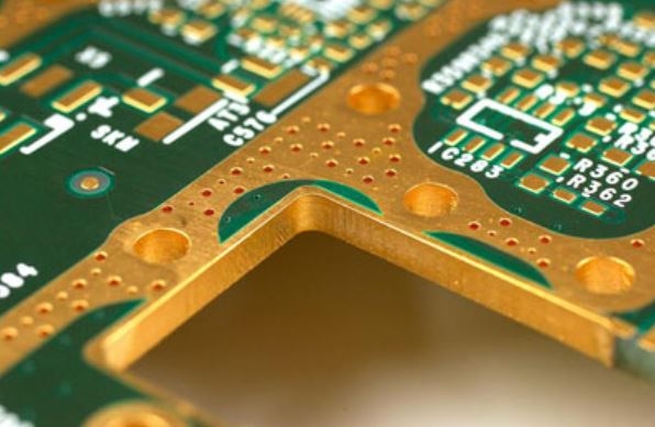
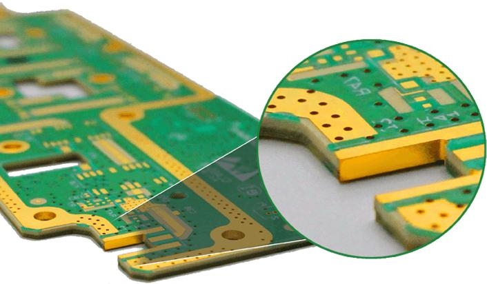
Plated edges refer to the metallic coating applied to the outer edges of a PCB, creating a conductive path or shield. In high-density PCBs, edge plating serves multiple purposes. It can act as a grounding mechanism to minimize electromagnetic interference (EMI), provide structural reinforcement, or facilitate connections in modular designs. The importance of edge plating in HDI boards lies in their compact nature, where space constraints demand innovative solutions for signal integrity and interference reduction.
Improperly designed plated edges can lead to manufacturing issues like uneven plating, delamination, or signal distortion. These problems are magnified in HDI PCBs due to tighter tolerances and multilayer configurations. By integrating DFM for edge plating early in the design phase, engineers can align their layouts with fabrication capabilities, ensuring consistent quality and performance. Addressing plated edges effectively also enhances the reliability of the final product in demanding applications.
Technical Principles of Edge Plating in High-Density PCBs
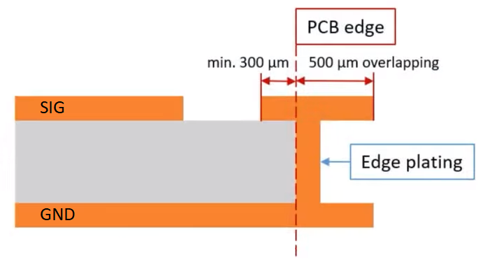
Edge plating in PCBs is achieved through a controlled electroplating process, where copper or other conductive materials are deposited along the board's perimeter. In HDI designs, this process must account for multilayer structures, microvias, and fine-pitch components. The primary technical aspects include ensuring uniform plating thickness, maintaining precise depth control, and managing impedance for signal integrity.
Controlled depth plating is critical to prevent overplating or underplating, which can affect the board's dimensions or electrical properties. This technique requires precise masking and process control during fabrication to limit plating to specific areas or depths. Impedance control for plated edges is equally important, especially in high-frequency applications. The conductive layer on the edge can influence signal paths, requiring careful calculation of trace geometry and dielectric properties to avoid mismatches.
Standards such as IPC-6012E provide guidelines for plating thickness and adhesion in rigid PCBs, ensuring that edge plating meets performance criteria. Adhering to these specifications helps mitigate risks like cracking or peeling during thermal cycles or mechanical stress. Engineers must also consider the material stack-up and edge preparation to achieve consistent results during manufacturing.
Challenges in Edge Plating for HDI PCBs
Implementing edge plating in high-density PCBs presents several challenges. One primary issue is achieving uniform plating across complex geometries. HDI boards often have irregular edges or cutouts, making it difficult to maintain consistent copper deposition. Variations in plating thickness can lead to weak spots, compromising EMI shielding or grounding effectiveness.
Another concern is the risk of defects during drilling or routing processes. Exposing inner layers for edge plating requires precise alignment, as misalignment can cause short circuits or open connections. Additionally, thermal expansion differences between the plating material and the PCB substrate may induce stress, leading to cracks or delamination over time.
Impedance control for plated edges adds another layer of complexity. In high-frequency designs, the plated edge can act as an unintended signal path, altering impedance characteristics. Engineers must model these effects during the design phase to prevent signal degradation. Addressing these challenges through robust DFM for edge plating is essential for successful HDI PCB production.
Practical Solutions and DFM Best Practices for Edge Plating
To overcome the challenges associated with edge plating in high-density PCBs, engineers must adopt targeted DFM strategies. Below are key best practices to ensure manufacturability and performance.
Define Clear Edge Plating Specifications
Start by specifying the areas requiring edge plating in the design files. Clearly indicate whether the plating should cover the entire edge or specific sections. Reference standards like IPC-A-600K for acceptability criteria on plating adhesion and coverage. Providing detailed documentation reduces ambiguity during fabrication.
Optimize Edge Preparation
Before plating, edges must be properly prepared through routing or milling to expose the necessary copper layers. Ensure that the design accounts for a smooth edge finish to avoid burrs or roughness that can disrupt plating uniformity. Collaborate with fabricators to confirm their capabilities for edge preparation.
Implement Controlled Depth Plating Techniques
For controlled depth plating, use precise masking to limit plating to designated areas. This approach prevents excessive copper buildup, which can interfere with board dimensions or assembly. Work within the tolerances outlined in IPC-6012E to maintain consistency across production batches.
Ensure Impedance Control for Plated Edges
In high-frequency HDI designs, impedance control for plated edges is vital. Calculate the impact of edge plating on signal paths using simulation tools. Adjust trace widths and spacing near plated edges to maintain desired impedance values. Incorporate ground planes or shielding layers to minimize interference.
Account for Thermal and Mechanical Stress
Select materials with compatible coefficients of thermal expansion to reduce stress at plated edges. Design adequate clearance around edge-plated areas to prevent mechanical damage during handling or assembly. Test prototypes under thermal cycling conditions to validate durability.
Minimize Design Complexity
Simplify edge geometries where possible to facilitate uniform plating. Avoid sharp corners or intricate cutouts that can complicate the plating process. Reducing complexity enhances manufacturing yield and lowers the risk of defects.
Testing and Validation for Edge Plating Quality
Validation is a critical step in ensuring the reliability of plated edges in HDI PCBs. Conduct visual inspections per IPC-A-600K to check for plating defects such as voids or uneven coverage. Use cross-sectional analysis to verify plating thickness and adhesion at the edges.
Electrical testing is also essential to confirm impedance control for plated edges. Measure characteristic impedance using time-domain reflectometry to detect mismatches caused by plating variations. Additionally, perform environmental stress tests, including thermal shock and humidity exposure, to assess long-term durability.
Document all test results and compare them against the performance criteria in IPC-6012E. This approach ensures that the edge plating meets industry standards and application requirements. Regular feedback loops with manufacturing teams can help refine DFM for edge plating over time.
Insight: Balancing Cost and Performance in Edge Plating
While edge plating enhances functionality in HDI PCBs, it can increase manufacturing costs due to additional processing steps. Engineers must balance performance needs with budget constraints. For instance, selective edge plating rather than full perimeter coverage can reduce material usage while still addressing EMI concerns.
Consider the end application when deciding on plating specifications. In less demanding environments, standard copper plating may suffice, avoiding the need for specialized finishes. Engage with fabrication partners early to understand cost drivers and explore cost-effective DFM for edge plating solutions without compromising quality.
Conclusion
Edge plating in high-density PCBs is a powerful technique for improving grounding, shielding, and structural integrity. However, its implementation demands careful attention to DFM principles to ensure manufacturability and performance. By focusing on controlled depth plating, impedance control for plated edges, and adherence to industry standards like IPC-6012E and IPC-A-600K, engineers can mitigate common challenges. Practical strategies such as clear specifications, optimized edge preparation, and rigorous testing are key to success. Applying these insights enables the creation of reliable HDI designs that meet the stringent requirements of modern electronics, ensuring both functionality and durability in critical applications.
FAQs
Q1: What is the purpose of plated edges in high-density PCBs?
A1: Plated edges in high-density PCBs serve to enhance grounding, reduce electromagnetic interference, and provide mechanical strength. They create a conductive path along the board's perimeter, crucial for signal integrity in compact designs. Adhering to DFM for edge plating ensures uniform application and prevents defects during manufacturing.
Q2: How does controlled depth plating improve edge plating in PCBs?
A2: Controlled depth plating limits copper deposition to specific areas or depths on PCB edges, preventing overplating or dimensional issues. This technique ensures consistency and reduces risks of short circuits in HDI layouts. Following standards like IPC-6012E helps maintain precision and reliability in the edge plating process.
Q3: Why is impedance control important for plated edges in HDI designs?
A3: Impedance control for plated edges is vital in high-frequency HDI designs to prevent signal distortion. Plated edges can alter signal paths, causing mismatches if not properly managed. Calculating trace geometry and incorporating shielding layers ensures stable performance, protecting the integrity of critical signals.
Q4: What standards guide DFM for edge plating in PCB manufacturing?
A4: Standards such as IPC-6012E for performance specifications and IPC-A-600K for acceptability criteria guide DFM for edge plating. These documents outline requirements for plating thickness, adhesion, and quality. Following them ensures manufacturability and reliability in high-density PCB production processes.
References
IPC-6012E — Qualification and Performance Specification for Rigid Printed Boards. IPC, 2020.
IPC-A-600K — Acceptability of Printed Boards. IPC, 2020.


