Introduction
Solder mask application is a critical step in printed circuit board (PCB) manufacturing, serving as a protective layer that insulates copper traces and prevents unintended solder connections during assembly. For electrical engineers, understanding the nuances of techniques like solder mask screen printing, spray coating, curtain coating, lamination, UV curing, development, and cleaning is essential for ensuring PCB reliability and performance. This guide explores each method in detail, offering technical insights into their processes, advantages, and best practices. By mastering these application techniques, engineers can optimize designs for durability and manufacturability while adhering to industry standards. Whether you are designing a high-density interconnects or heavy copper PCB, this article provides a comprehensive roadmap to achieving a robust solder mask layer.
What Is Solder Mask and Why It Matters
Solder mask, often referred to as solder resist, is a thin polymer coating applied to the surface of a PCB. Its primary function is to protect copper traces from oxidation, prevent solder bridges during component assembly, and insulate conductive paths to avoid short circuits. Beyond protection, it also enhances the aesthetic appeal of the board by providing a uniform color, typically green, though other colors are available based on design needs.
The importance of solder mask in PCB manufacturing cannot be overstated. It directly impacts the board's longevity, reliability, and performance in harsh environments. A poorly applied solder mask can lead to defects like incomplete coverage, pinholes, or adhesion failures, resulting in costly rework or field failures. For electrical engineers, selecting the right application technique and ensuring process control are vital to meeting stringent quality requirements, especially in applications like aerospace, automotive, and medical devices where reliability is paramount.
Technical Principles of Solder Mask Application
Solder mask application involves depositing a protective layer onto the PCB surface using various methods, each with distinct mechanisms. The choice of technique depends on factors such as board complexity, production volume, and material properties. Below, we outline the core principles behind each method, focusing on their technical foundations.
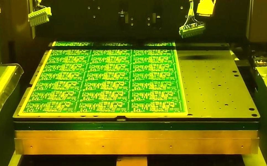
Solder Mask Screen Printing
Solder mask screen printing is one of the most traditional and widely used methods. It involves using a mesh screen with a stencil to apply liquid solder mask ink onto the PCB surface. The screen is aligned over the board, and ink is forced through the mesh using a squeegee, covering areas where copper traces need protection while leaving pads and vias exposed.
This method relies on precise alignment and ink viscosity to ensure uniform coverage. It is cost-effective for low to medium volume production and works well for simpler designs. However, it may struggle with fine-pitch components due to limitations in resolution.
Solder Mask Spray Coating
Spray coating applies solder mask material as a fine mist using pressurized nozzles. The PCB is passed through a spray system, allowing for even distribution of the coating across complex geometries. This technique is ideal for boards with intricate designs or high-density features, as it can reach areas that screen printing might miss.
The process requires careful control of spray pressure and nozzle distance to avoid overspray or uneven thickness. It is often used in automated, high-volume production settings due to its speed and consistency.
Solder Mask Curtain Coating
Curtain coating involves passing the PCB under a continuous stream or “curtain” of liquid solder mask material. The board moves on a conveyor, and the material flows over it, creating a uniform layer. Excess material is collected and recycled, making this method efficient for large-scale production.
This technique excels in achieving consistent thickness across the board surface. It is less suited for selective application, as it coats the entire board, requiring additional steps to expose specific areas like pads.
Solder Mask Lamination
Lamination uses a dry film solder mask, which is a pre-formed sheet of photoimageable material. The film is applied to the PCB surface under heat and pressure, bonding it to the board. After lamination, the film is exposed to light through a photomask to define protected and exposed areas.
This method offers high precision and is commonly used for complex designs requiring fine detail. It aligns with processes governed by standards like IPC-A-600K for acceptability of printed boards.
Post-Application Processes
After the initial application, solder mask undergoes several critical steps to finalize the protective layer. These processes ensure adhesion, durability, and functionality of the coating.
Solder Mask UV Curing
UV curing is a pivotal step for photoimageable solder masks, whether applied via lamination or liquid methods. The coated PCB is exposed to ultraviolet light, which triggers a chemical reaction in the mask material, hardening it into a solid layer. Areas not intended to be cured are protected by a photomask during exposure.
This process demands precise control of light intensity and exposure time to avoid under-curing or over-curing, which could compromise the mask's integrity. It aligns with quality benchmarks outlined in IPC-6012E for rigid printed boards.
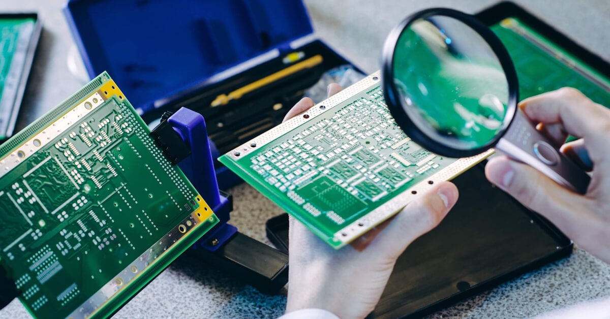
Solder Mask Development
Development follows UV curing for photoimageable masks. The PCB is immersed in a chemical solution that removes uncured material from areas like pads and vias, exposing them for soldering. The developer solution must be carefully formulated to avoid damaging the cured mask.
This step is critical for achieving accurate openings and requires strict adherence to process parameters to prevent defects like residual mask on pads. It ties directly to standards such as IPC-A-600K for ensuring acceptability.
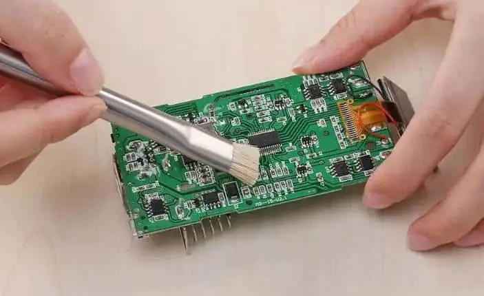
Solder Mask Cleaning
Cleaning is the final step, removing any residues, contaminants, or excess material from the PCB surface after development. This process typically involves rinsing with deionized water or specialized cleaning agents to ensure no chemical traces remain that could affect soldering or long-term reliability.
Proper cleaning prevents issues like poor adhesion of surface finishes or contamination during assembly. It is a key aspect of quality control, aligning with guidelines in IPC-6012E for performance specifications.
Suggested Reading: Understanding Solder Mask: A Beginner's Guide to PCB Protection
Practical Solutions and Best Practices
Achieving a durable and effective solder mask layer requires attention to detail at every stage. Below are actionable best practices for electrical engineers to optimize each technique.
- Screen Printing Precision: Ensure stencil alignment is verified before application. Use inks with consistent viscosity to avoid uneven coverage. Regularly inspect screens for wear to maintain resolution.
- Spray Coating Control: Calibrate spray equipment to maintain uniform pressure and distance. Implement masking for areas not requiring coating to prevent overspray on critical features.
- Curtain Coating Consistency: Monitor conveyor speed and material flow rate to achieve even thickness. Test samples periodically to confirm compliance with thickness specifications per IPC-A-600K.
- Lamination Accuracy: Apply uniform heat and pressure during lamination to prevent air bubbles or delamination. Validate photomask alignment to ensure precise exposure of pads.
- UV Curing Optimization: Use calibrated UV lamps and monitor exposure time to achieve full curing. Test cured masks for hardness and adhesion to confirm process stability.
- Development Monitoring: Control developer solution concentration and temperature. Inspect boards post-development for residue or incomplete removal using visual and automated inspection methods.
- Cleaning Thoroughness: Use high-purity water or approved agents for cleaning. Implement drying processes to eliminate moisture that could lead to corrosion.
Troubleshooting Common Solder Mask Issues
Even with robust processes, issues can arise during solder mask application. Below are common problems and their solutions, tailored for electrical engineers seeking practical fixes.
- Pinholes in Mask: Often caused by contamination or air bubbles during application. Ensure cleanroom conditions and degas liquid materials before use. For screen printing, check squeegee pressure.
- Incomplete Curing: Results from insufficient UV exposure. Verify lamp intensity and exposure duration. Replace aging lamps to maintain consistent curing as per IPC-6012E guidelines.
- Mask Adhesion Failure: Typically due to surface contamination or improper curing. Enhance pre-application cleaning and confirm curing parameters. Test adhesion using standardized methods.
- Residue After Development: Indicates improper developer concentration or dwell time. Adjust solution parameters and inspect rinse effectiveness to ensure clean surfaces.
Conclusion
Solder mask application is a cornerstone of PCB manufacturing, directly influencing board reliability and performance. Techniques like solder mask screen printing, spray coating, curtain coating, lamination, UV curing, development, and cleaning each offer unique advantages suited to different design and production needs. By understanding the technical principles and adhering to best practices, electrical engineers can mitigate risks of defects and ensure compliance with industry standards. A methodical approach to process control, from application to final cleaning, guarantees a robust protective layer, paving the way for high-quality PCBs in demanding applications.
FAQs
Q1: What are the advantages of solder mask screen printing over other methods?
A1: Solder mask screen printing is cost-effective for low to medium volume production and simpler PCB designs. It requires minimal equipment investment compared to automated methods like spray coating. However, it may lack precision for fine-pitch components. Engineers should select this method when budget and design simplicity are priorities, ensuring stencil alignment for optimal results.
Q2: How does solder mask spray coating benefit complex PCB designs?
A2: Solder mask spray coating excels in covering intricate geometries and high-density boards due to its ability to apply a fine, even layer. It reaches areas that screen printing might miss, making it ideal for advanced designs. Engineers must control spray parameters to avoid overspray, ensuring uniform thickness for reliability in demanding applications.
Q3: What factors should be monitored during solder mask UV curing?
A3: During solder mask UV curing, engineers must monitor light intensity, exposure time, and lamp condition to ensure complete hardening of the mask. Insufficient curing can lead to adhesion issues, while over-curing may cause brittleness. Regular calibration of equipment and adherence to standards like IPC-6012E are crucial for consistent outcomes.
Q4: Why is solder mask cleaning critical after development?
A4: Solder mask cleaning removes chemical residues and contaminants post-development, preventing issues like poor surface finish adhesion or soldering defects. Using high-purity water or approved agents ensures no traces remain that could affect long-term reliability. This step aligns with quality specifications in standards like IPC-A-600K for acceptable PCB surfaces.
References
IPC-6012E — Qualification and Performance Specification for Rigid Printed Boards. IPC, 2020.
IPC-A-600K — Acceptability of Printed Boards. IPC, 2020.


