Introduction
Wave soldering remains a cornerstone process for through-hole PCB assembly, particularly for components requiring robust mechanical connections. Achieving consistent PCB wave soldering hole fill ensures reliable electrical performance and structural integrity in demanding applications. Engineers often face challenges like incomplete barrel filling or excessive solder wicking, which can compromise joint quality. Understanding the interplay of process parameters, board design, and material properties is essential for optimization. This article explores practical techniques to enhance PCB wave soldering plated through hole performance while adhering to established industry benchmarks.
Understanding Hole Fill in PCB Wave Soldering
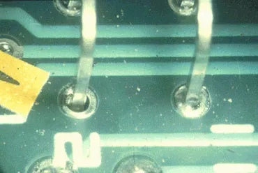
Hole fill refers to the extent to which molten solder completely occupies the plated through hole (PTH) barrel during wave soldering, forming a solid joint upon cooling. Inadequate fill leads to voids or weak interconnections, potentially causing failures under thermal stress or vibration. Consistent PCB wave soldering hole fill directly impacts assembly yield and long-term reliability, making it a critical metric for electric engineers. Factors such as capillary action drive solder upward into the hole, but imbalances can result in defects like solder balls or bridging. Proper evaluation aligns with acceptability criteria outlined in IPC-A-610, ensuring joints meet performance expectations across classes.
Why Consistent Hole Fill Matters
Reliable hole fill prevents intermittent connections that degrade signal integrity in high-frequency circuits. It also enhances thermal dissipation by minimizing air gaps within the PTH, crucial for power electronics. Poor fill exacerbates issues like solder wicking, where solder preferentially climbs component leads rather than filling the barrel. This not only weakens the joint but increases the risk of cracking during board flexure. For electric engineers, mastering PCB wave soldering via fill translates to fewer rework cycles and higher production throughput. Ultimately, it supports compliance with soldering requirements in J-STD-001, fostering dependable assemblies in automotive and industrial environments.
Technical Principles Governing Hole Fill
Capillary action is the primary mechanism propelling molten solder into the PTH during wave soldering, governed by surface tension and wetting angle between solder, plating, and flux residues. The narrow annular gap between the component lead and hole wall creates a capillary rise, but high aspect ratios or contaminated surfaces hinder flow. Solder viscosity decreases with temperature, facilitating better penetration, while flux removes oxides to promote wetting. Excessive capillary action can lead to PCB wave soldering solder wicking, drawing solder upward along leads and starving the barrel. Engineers must balance these dynamics through controlled preheat and immersion times. Plating quality, such as electroless nickel immersion gold or HASL, influences initial wettability, setting the stage for uniform fill.
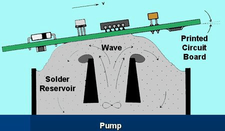
Wave dynamics play a pivotal role, with the solder wave's laminar flow ensuring even contact across the board underside. Turbulent waves disrupt capillary flow, causing inconsistent PCB wave soldering plated through hole results. Dwell time in the wave, determined by conveyor speed, allows sufficient opportunity for solder to climb the barrel. Thermal gradients from board thickness affect local viscosity, potentially leading to shadowed areas on denser panels. Preheat profiles activate flux evenly, preventing dewetting in deeper holes. These principles underscore the need for process tuning to counteract natural capillary forces.
Key Factors Affecting Hole Fill Performance
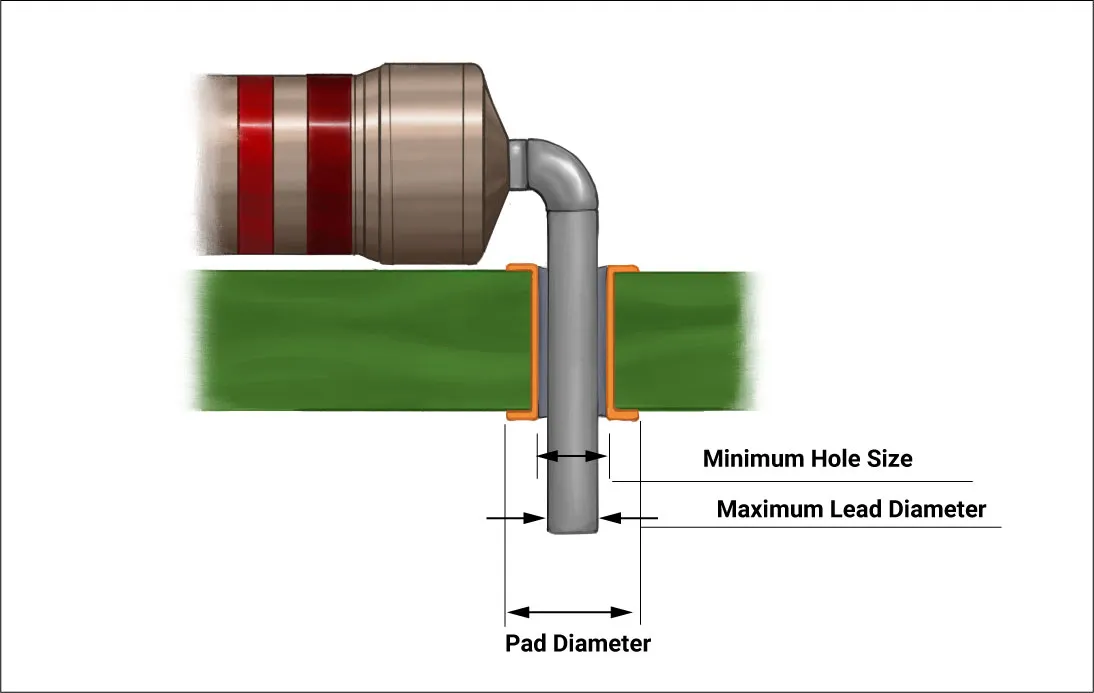
Board design significantly influences PCB wave soldering via fill, particularly hole diameter relative to board thickness and lead protrusion length. Oversized holes delay capillary rise, while tight fits promote wicking if leads are misaligned. Component lead form, such as straight versus formed, alters flow paths and can trap air pockets. Flux selection is critical; alcohol-based fluxes with low solids content penetrate holes effectively without excessive residue. Solder alloy composition affects surface tension, with lead-free options requiring higher temperatures for comparable flow.
Process parameters further modulate outcomes. Inadequate preheat fails to expand the board uniformly, impeding flux activation and solder fluidity. Conveyor speed too fast reduces immersion time, resulting in partial fills. Wave height must contact pads without flooding, avoiding bridging while ensuring barrel entry. Board warpage exacerbates uneven wetting, as bowed panels lift edges from the wave. Cleanliness of incoming boards prevents contamination that blocks capillary channels.
Best Practices for Achieving Consistent Hole Fill
Optimize preheat to achieve uniform board temperature, promoting flux volatilization and solder wetting without overheating components. Profiles typically ramp gradually to avoid thermal shock, ensuring holes are flux-primed before wave contact. Select fluxes designed for wave soldering that exhibit strong hole penetration and minimal stringing. Apply via spray or foam for even coverage, verifying activation through top-side inspection.
Adjust conveyor speed to provide 3-5 seconds of wave dwell, allowing capillary action to complete barrel fill. Lower speeds for thicker boards compensate for higher thermal mass. Maintain solder pot temperature to balance viscosity and dross formation, with regular skimming to preserve alloy purity. Implement board fixturing to minimize warpage, supporting panels flat against the wave. Nitrogen blanketing reduces oxidation, enhancing wetting on lead-free assemblies.
Lead preparation is vital; trim and form components to specified protrusion, typically 1.5-2 times hole diameter for optimal flow. This ensures solder reaches the top-side pad without excess wicking. Post-solder cooling under controlled airflow solidifies joints uniformly, preventing cracks. Regular process audits, including cross-section analysis, verify compliance with IPC J-STD-001 criteria. These techniques collectively yield repeatable PCB wave soldering hole fill.
Troubleshooting Common Hole Fill Defects
Insufficient barrel fill often stems from poor fluxing or low preheat, manifesting as concave menisci or voids. Increase preheat soak time and verify fluxer nozzle alignment for better penetration. Solder wicking, driven by PCB wave soldering capillary action imbalance, appears as fillet depletion on leads. Mitigate by optimizing lead protrusion and using anti-wick fluxes. Bridging between adjacent pins results from excessive wave height; reduce immersion depth and increase speed incrementally.
Voids from trapped flux gases require improved venting through slower ramps or vacuum-assisted waves. Icicles form from dripping solder post-exit; clean pallets and adjust drag-out angles. For persistent issues, inspect plating integrity per solderability tests. Cross-section sampling pinpoints root causes like plating cracks inhibiting wetting. Systematic adjustments restore consistency.
Advanced Techniques for Challenging Assemblies
Thick boards or high-density designs demand selective wave soldering for targeted PTH exposure, minimizing shadowing. Dual-wave setups with turbulent first wave for fluxing and laminar second for filling enhance results. Aspect ratios exceeding standard limits benefit from extended protrusion or plugged vias to direct flow. Integration with automated optical inspection flags early defects, enabling real-time tweaks.
Conclusion
Consistent PCB wave soldering hole fill hinges on harmonizing design, materials, and process controls to leverage capillary action effectively. Practical steps like precise preheating, flux optimization, and parameter tuning deliver robust joints compliant with industry standards. Electric engineers can troubleshoot defects methodically, from wicking to voids, boosting assembly reliability. Implementing these tips reduces variability, ensuring high-yield production. Prioritize cross-verification to sustain performance in evolving applications.
FAQs
Q1: What causes insufficient hole fill in PCB wave soldering plated through hole processes?
A1: Insufficient fill typically arises from inadequate flux penetration, low preheat temperatures, or excessive conveyor speeds that limit dwell time. Contaminated hole walls or poor plating wettability further impede capillary flow. Engineers should audit flux application and thermal profiles first. Adjusting these parameters often restores 100% barrel fill without major redesigns.
Q2: How does PCB wave soldering capillary action contribute to solder wicking?
A2: Capillary action draws solder into narrow gaps, but preferential wetting on leads over the barrel causes wicking. This imbalance occurs with excessive lead protrusion or thermal mismatches. Mitigate by standardizing lead lengths and using low-residue fluxes. Proper preheat equalizes surfaces, directing flow into the PTH effectively.
Q3: What are key design tips for better PCB wave soldering via fill?
A3: Maintain favorable hole-to-board thickness aspect ratios and adequate pad annular rings to support solder rise. Ensure lead protrusion aligns with process windows for complete wetting. Avoid dense clustering that shadows waves. These design choices complement process controls for reliable fill.
Q4: How can engineers verify consistent PCB wave soldering hole fill?
A4: Use cross-section metallography on sample boards to measure barrel occupancy against criteria. Visual inspection per IPC-A-610 checks for voids or concavity. Automated X-ray reveals internal defects non-destructively. Regular verification refines processes proactively.
References
IPC-A-610H — Acceptability of Electronic Assemblies. IPC, 2019
IPC J-STD-001G — Requirements for Soldered Electrical and Electronic Assemblies. IPC, 2017
J-STD-003D — Solderability Tests for Printed Boards. IPC, 2020