Introduction
High-speed digital circuits demand precise control over signal propagation to maintain data integrity at multi-gigabit speeds. In multilayer printed circuit boards, plated through-holes often leave conductive stubs that extend beyond the active signal layers, causing impedance discontinuities and reflections. PCB back drilling methods address this by selectively removing these stubs, enhancing overall performance. This technique has become essential in advanced back drilling applications for servers, telecommunications, and computing systems. Engineers must understand its principles to optimize via structures effectively. As designs push beyond 10 Gbps, via optimization through backdrilling directly impacts eye diagram quality and bit error rates.
What Is PCB Back Drilling and Why It Matters for High-Speed Digital Design
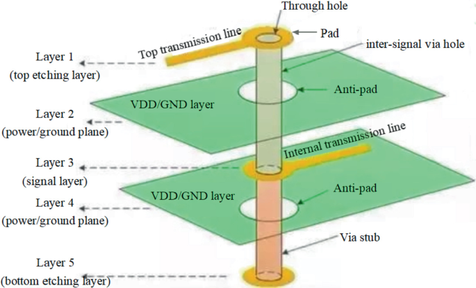
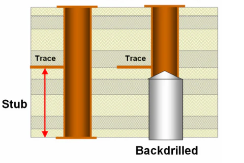
PCB back drilling, also known as controlled depth drilling, involves drilling out the unused portion of a plated through-hole from the opposite side of the board after initial via formation. This process targets the via stub, the copper-plated section extending past the innermost layer used by the signal, which acts as a resonant transmission line stub. In high-speed digital design, these stubs introduce return loss and insertion loss, degrading signal integrity techniques like equalization and pre-emphasis. Without backdrilling, signals experience ringing and crosstalk, limiting channel margins. The relevance grows with layer counts exceeding 20, where through-vias dominate routing. Adopting advanced back drilling ensures compliance with performance specs in dense interconnects.
Backdrilling matters because conventional blind or buried vias increase fabrication costs exponentially with layer depth. It provides a cost-effective alternative for non-critical nets while preserving full-layer connectivity. Signal simulations reveal stub lengths as short as a few millimeters can resonate at frequencies above 5 GHz, necessitating removal for clean eye openings. Industry shifts toward 112 Gbps PAM4 signaling amplify this need, making backdrilling a staple in signal integrity techniques. Engineers benefit from shorter design cycles without redesigning stackups solely for via types.
Technical Principles Behind Backdrilling
The core principle of backdrilling relies on precise depth control to excise the stub while preserving the barrel at the target layer. Initial through-hole drilling and plating create a continuous conductor across all layers. A larger-diameter drill, typically offset by 0.1 to 0.2 mm, enters from the backside to remove plating up to just above the landing pad, leaving a clean shoulder. This minimizes the effective stub length to near zero, aligning via impedance with trace characteristics. Reflections diminish as the stub's electrical length falls below one-tenth of the signal wavelength. Time-domain reflectometry confirms the improvement through reduced echo amplitude.
Electromagnetic field behavior around the via changes post-backdrill, with fields confining more to the active barrel. Parasitic capacitance and inductance drop, smoothing transitions for differential pairs. In high-speed contexts, this supports SerDes channels by lowering bit error rates under crosstalk stress. Depth accuracy hinges on panel flatness, drill peck cycles, and entry board materials to avoid wander. Verification coupons on panels, as per IPC-6012 standards, measure stub remnants via cross-sectioning or capacitance testing. These principles extend to staggered backdrills for multiple stub zones in asymmetric stackups.
Advanced PCB Back Drilling Methods
Advanced back drilling evolves beyond single-depth removal to handle complex multilayer boards. Stepped backdrilling applies sequential drills at varying depths for vias spanning multiple signal groups, optimizing each segment independently. This method suits HDI boards where inner layers host mixed-speed nets. Engineers specify backdrill pairs in fabrication drawings, pairing entry-exit sides with nominal depths and tolerances. Multi-step processes reduce overall stub impact by 80 percent or more in simulations, though alignment precision is critical.
Controlled depth variations incorporate peck drilling to evacuate chips, preventing heat buildup and wander in thick cores. Hybrid approaches combine backdrilling with laser ablation for ultra-fine stubs under 0.5 mm, though mechanical drilling dominates for scalability. Signal integrity techniques integrate backdrill planning during routing, using field solvers to predict resonance peaks. For symmetric boards, mirrored backdrills from both sides halve individual drill depths, easing tolerances. These methods demand CAM software validation to generate unique drill files per step.
Via-in-pad backdrilling targets filled vias, removing outer stubs while retaining fill integrity for thermal management. Depth zoning classifies nets by speed: critical high-speed digital design vias get full stub excision, while slower ones retain partial barrels. Tolerances tighten to ±50 microns for 56 Gbps PAM4, verified via X-ray or electrical testing. Advanced setups use optical alignment for panel fiducials, ensuring repeatability across production runs.
Best Practices for Via Optimization and Signal Integrity Techniques
Start via optimization by simulating full channel models including backdrilled vias early in high-speed digital design. Assign backdrill depths based on stub resonance frequency, targeting lengths under a quarter-wavelength at the knee frequency. Collaborate with fabricators on drill size margins to balance stub clearance and pad annular ring preservation. Incorporate verification nets in stackup margins for inline testing. IPC-A-600 guidelines define acceptable shoulder geometry post-drill, guiding inspection criteria.
Layout strategies cluster backdrilled vias away from power planes to minimize coupling. Use anti-pad expansions matching drill offsets to prevent breakthrough. For differential pairs, symmetric backdrilling maintains balance, crucial for common-mode rejection. Post-fabrication, electrical S-parameters validate improvements, correlating to eye height gains. Layer sequencing favors signal layers near surfaces for minimal stubs without backdrill. These practices integrate seamlessly into DFM checks.
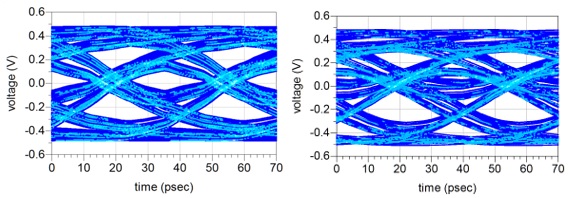
Table 1: Key Backdrill Parameters for Optimization
- Drill Diameter Oversize: 0.10-0.25 mm larger than PTH — Ensure stub removal without pad damage
- Depth Tolerance: ±0.10 mm typical — Maintain landing pad integrity
- Minimum Shoulder: 0.15 mm — Prevent electrical short
- Verification Method: Cross-section coupons — Confirm stub length
Challenges and Troubleshooting in Advanced Backdrilling
Warpage in thick panels complicates depth uniformity, requiring bake cycles or carriers during drilling. Excessive chip load leads to rough shoulders, increasing capacitance; mitigate with optimized feed rates. Misalignment from drill wander hits active barrels, causing opens; fiducial registration counters this. Troubleshooting starts with panel coupons: if stub remnants exceed specs, adjust peck depth or spindle speed. Aspect ratios over 15:1 challenge evacuation, risking smear.
For high-speed digital design, residual stubs manifest as specific frequency nulls in insertion loss plots. Cross-section analysis per IPC-6012 reveals common defects like dog-boning or plating voids. Multi-step backdrills risk cumulative tolerances; simulate worst-case stackups. Production yields improve with pilot runs on scrap panels. Engineers document lessons in fab notes for iterative refinement.
Conclusion
Advanced PCB back drilling techniques revolutionize signal integrity in high-speed digital circuits by eliminating via stub impediments. From basic controlled depth removal to stepped methods, these approaches enable robust via optimization without exorbitant blind via costs. Engineers achieve superior performance through simulation-driven planning and precise fabrication controls. Adhering to standards ensures reliability across volumes. As data rates escalate, backdrilling remains a cornerstone of effective PCB back drilling methods.
FAQs
Q1: What are the primary PCB back drilling methods for high-speed digital design?
A1: PCB back drilling methods include single-depth drilling for uniform stubs, stepped backdrilling for multi-zone removal, and hybrid laser-mechanical for fine control. Each targets via stubs causing reflections, with drill diameters oversized to clear plating cleanly. Depth control relies on peck cycles and fiducials. These methods integrate into CAM workflows for signal integrity techniques, verified via coupons. Selection depends on layer count and speed requirements.
Q2: How does advanced back drilling improve signal integrity techniques?
A2: Advanced back drilling removes conductive stubs, reducing impedance mismatches and resonances in high-speed paths. This lowers insertion and return loss, enhancing eye margins for multi-Gbps signals. Simulations predict gains before fab, guiding depth specs. Combined with routing optimization, it supports longer channels without repeaters. Verification confirms stub lengths near zero, aligning with design goals.
Q3: What role does via optimization play in PCB back drilling methods?
A3: Via optimization in PCB back drilling methods involves classifying nets by speed, assigning targeted stub removals, and balancing drill tolerances with annular rings. High-speed digital design vias prioritize full excision, while others use partial. This minimizes parasitics, aiding crosstalk immunity. Stackup planning clusters critical vias for efficiency. Results yield flatter frequency responses across bands.
Q4: When should electrical engineers consider backdrilling in high-speed designs?
A4: Consider backdrilling when through-vias exceed stub lengths risking resonance at operating frequencies, typically above 3 Gbps. It's ideal for cost-sensitive multilayer boards over 12 layers. Simulate channels first to quantify benefits versus blind vias. Fab DFM reviews confirm feasibility. It excels in symmetric stackups for uniform depths.
References
IPC-6012E — Qualification and Performance Specification for Rigid Printed Boards. IPC, 2017
IPC-A-600K — Acceptability of Printed Boards. IPC, 2020
IPC-2221B — Generic Standard on Printed Board Design. IPC, 2012