Introduction
In multilayer PCB manufacturing, ensuring robust interlayer connections is critical for overall board reliability, especially as designs push toward higher densities and faster signal speeds. PCB etch back techniques remove excess dielectric material from via walls, exposing inner layer copper to enhance plating adhesion and electrical continuity. Traditional chemical methods have limitations in precision and environmental impact, making plasma etching an advanced alternative. This process uses ionized gases to achieve controlled material removal without aggressive wet chemistries. For electric engineers working on high-speed PCB designs, understanding plasma-based PCB etch back can significantly improve via connection integrity and long-term performance. This article explores the principles, benefits, and best practices of plasma etching in multilayer PCB production.
Understanding PCB Etch Back and Its Role in Multilayer PCBs
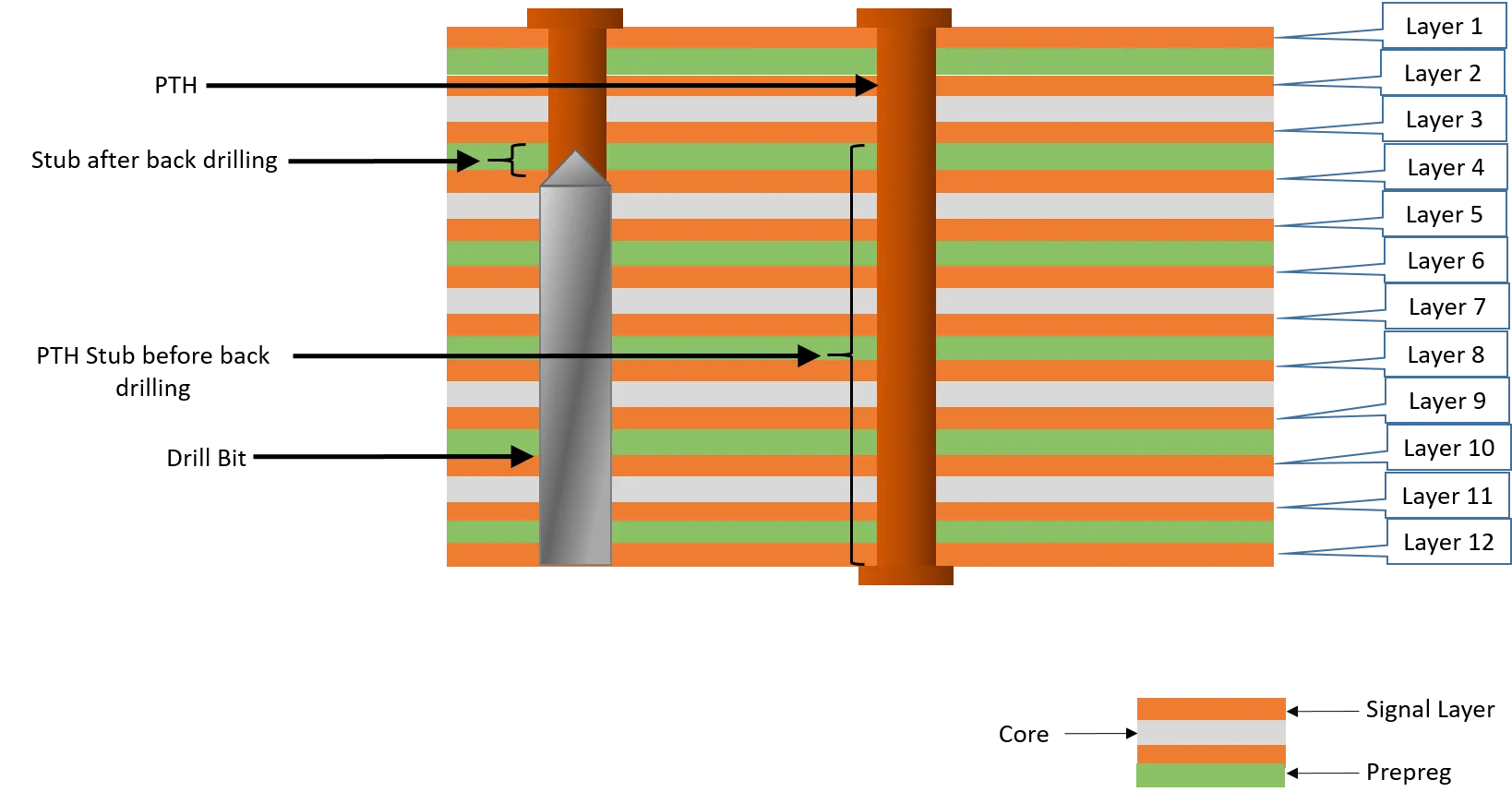
PCB etch back, often performed after drilling and desmearing, intentionally recesses the epoxy resin from plated through-hole sidewalls to reveal a controlled amount of inner layer copper. This step is essential in multilayer PCB fabrication where vias serve as critical interlayer connections, carrying high-frequency signals prone to integrity issues if not properly formed. Without adequate etch back, smear residues or poor copper exposure can lead to plating voids, increasing resistance and failure risks under thermal stress. Plasma etching stands out for its ability to perform both desmear and etch back in a single, dry process, offering superior uniformity across panel sizes. In high-reliability applications, such as those governed by IPC-6013 standards, precise etch back ensures the necessary copper exposure for mechanical and electrical robustness. Engineers designing high-speed PCBs benefit from this technique as it minimizes impedance discontinuities at vias.
The process matters because modern multilayer PCBs demand tighter tolerances for via connection reliability. As layer counts increase, even minor defects in interlayer bonds can propagate failures during assembly or operation. Plasma methods address these challenges by providing anisotropic etching, which targets vertical walls more effectively than isotropic chemical baths.
Technical Principles of Plasma Etching for PCB Etch Back
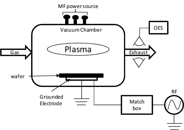
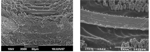
Plasma etching generates a low-pressure glow discharge where gases like oxygen or fluorocarbon mixtures become ionized, producing reactive species such as atomic oxygen and fluorine radicals. These species interact with the dielectric surface in the via, breaking polymer chains into volatile byproducts that evacuate the chamber without residue. The physical component involves ion bombardment, enhancing etch rates and directionality, while chemical reactions dissolve the epoxy selectively. Key parameters include RF power for plasma density, chamber pressure typically below 10 Pa for mean free path control, and gas flow rates to maintain chemistry balance. For PCB etch back, oxygen-rich plasmas excel at organic removal, while adding CF4 introduces fluorine for faster resin recession.
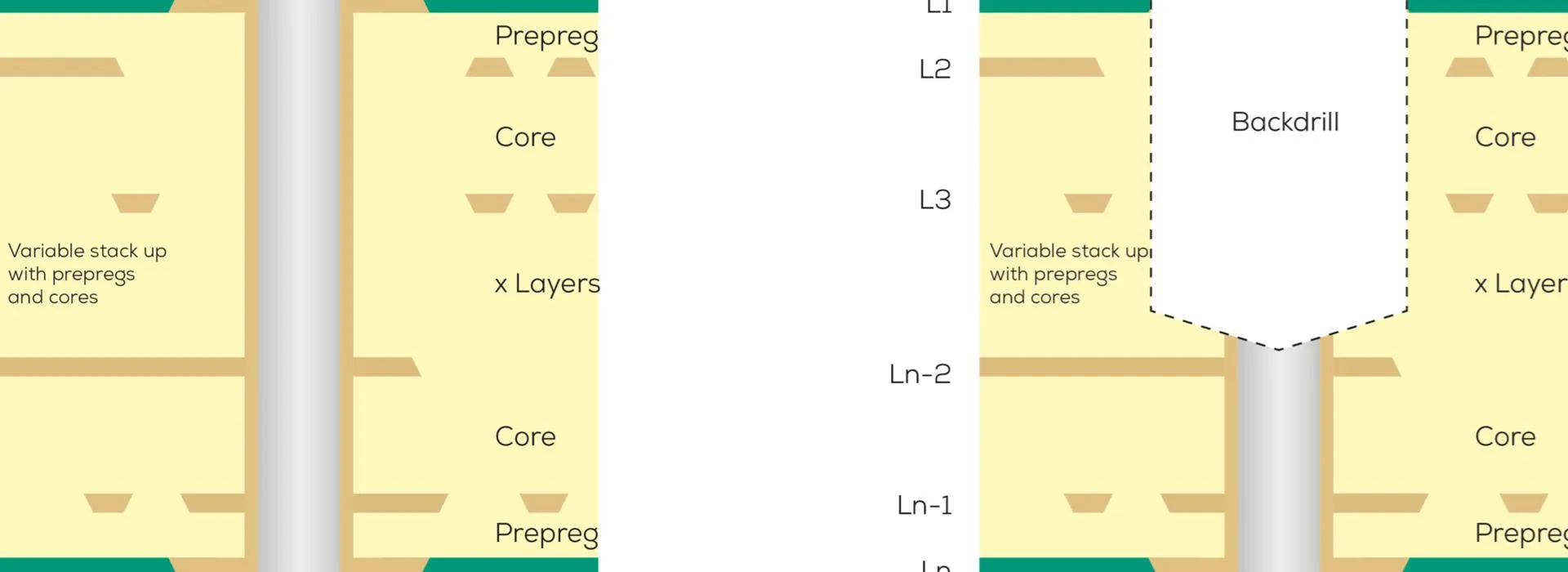
In practice, the process sequence starts with panel loading into a vacuum chamber, followed by pump-down and gas introduction. Etch uniformity depends on electrode configuration, often using barrel or downstream reactors for large panels. Electric engineers appreciate the scalability, as plasma systems handle high-volume production while allowing recipe tweaks for specific laminate types. Cross-sections reveal the etch profile: a smooth, tapered recess exposing 0.001 to 0.003 inches of copper, aligning with qualification requirements.
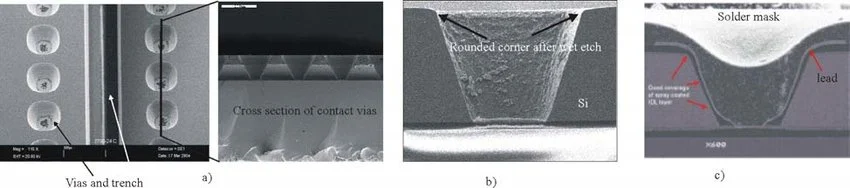
The mechanism's precision stems from the plasma sheath, where ions accelerate perpendicularly to the surface, minimizing lateral undercutting. This is vital for high-speed PCB design, where via stubs must maintain consistent geometry to avoid signal reflections.
Advantages of Plasma Etching Over Traditional Methods
Plasma etching surpasses chemical permanganate desmear by eliminating hazardous waste and rinse steps, reducing environmental footprint in factory operations. It achieves deeper penetration into fine vias without swelling the resin, a common issue with wet processes that can crack glass fibers. For via connection reliability, plasma ensures complete smear removal and controlled etch back, fostering stronger electroless copper adhesion during subsequent plating. In multilayer PCBs, this translates to fewer drill smear-induced opens, enhancing yield in complex stackups.
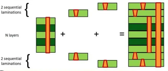
Reliability gains are evident in thermal cycling and vibration tests, where plasma-treated vias show superior barrel pull strength. High-speed PCB designs benefit from reduced via capacitance variations, supporting impedance control at GHz frequencies. Factories report consistent results across panel areas, unlike chemical baths prone to concentration gradients. Overall, plasma integrates seamlessly into sequential lamination workflows for advanced builds.
Best Practices for Implementing Plasma Etch Back in Production
Start with panel preparation: clean drilled boards to remove debris, then optimize plasma recipes based on laminate resin content. Use oxygen for initial desmear, transitioning to O2/CF4 blends for etch back to balance speed and selectivity. Monitor endpoints via optical emission spectroscopy for reactive species peaks, preventing over-etch that could thin inner foils. Maintain vacuum integrity and rotate panels in planetary systems for uniformity on large formats.
Post-etch inspection per IPC-TM-650 methods confirms copper exposure via cross-sectioning or resistivity checks. For high-speed multilayer PCB designs, pair etch back with controlled depth drilling to minimize stub lengths. Factory engineers should validate processes on qualification lots, adjusting power from 200-800 W and exposure times up to 60 minutes based on via aspect ratios. Integrate black hole treatments beforehand for carbon-rich laminates to enhance plasma efficacy.
Troubleshooting common issues involves recipe iteration: uneven etch signals high gas flow asymmetry, addressed by manifold redesigns. Over-etch appears as haloing; mitigate with lower bias voltages. These practices ensure via connection reliability meets IPC-6012 performance specs for rigid boards.
Challenges and Mitigation Strategies
One challenge is handling high-aspect-ratio vias in dense multilayer PCBs, where plasma diffusion limits may cause bottom smear persistence. Downstream plasma configurations with longer residence times resolve this, distributing radicals evenly. Cost concerns arise from vacuum equipment, but throughput gains offset investments in high-volume lines. Material variability, like high-Tg resins, demands adaptive chemistries to avoid underperformance.
For high-speed designs, excessive etch back risks copper dissolution; precise control via mass spectrometry feedback loops prevents this. Factories mitigate contamination by scheduling clean cycles with argon purges. Overall, plasma's dry nature simplifies integration, boosting reliability without compromising throughput.
Conclusion
Plasma etching revolutionizes PCB etch back by delivering precise, environmentally sound control over dielectric recess in multilayer PCBs. This technique fortifies via connections, elevating reliability for demanding high-speed applications. Electric engineers gain actionable insights into parameters and practices that align with industry benchmarks like IPC standards. Adopting plasma methods enhances interlayer integrity, reduces defects, and supports evolving design complexities. Factories implementing these advanced processes position themselves for superior quality and performance.
FAQs
Q1: What is PCB etch back and why is it essential for multilayer PCB reliability?
A1: PCB etch back recesses dielectric from via walls to expose inner copper, improving plating adhesion and electrical continuity. In multilayer PCBs, it prevents smear-induced failures under thermal stress, ensuring robust interlayer connections. This is critical for high-reliability per IPC-6013, minimizing resistance rises that degrade signal integrity. Plasma variants offer uniform results, vital for complex stackups.
Q2: How does plasma etching improve via connection in high-speed PCB design?
A2: Plasma etching provides anisotropic removal, creating clean via profiles that enhance copper plating wraparound. This reduces impedance mismatches and capacitance at vias, preserving signal speeds in high-speed designs. Compared to chemicals, it avoids resin swelling, boosting mechanical strength for thermal cycling. Uniformity across panels supports dense routing without defects.
Q3: What are key parameters for effective plasma etching in PCB etch back?
A3: Critical parameters include RF power for ion energy, low chamber pressure for directionality, and gas mixes like O2/CF4 for resin selectivity. Exposure times scale with via aspect ratios, monitored via spectroscopy. These ensure controlled copper exposure without over-etch, aligning with standards for via reliability in multilayer boards.
Q4: When should plasma etching be specified over chemical methods for multilayer PCBs?
A4: Opt for plasma in high-reliability or fine-pitch multilayer PCBs needing precise etch back and minimal waste. It excels in environmental compliance and uniformity for high-speed designs, avoiding chemical-induced microcracks. Specify per IPC guidelines when via connection integrity demands exceed wet process capabilities.
References
IPC-6012E — Qualification and Performance Specification for Rigid Printed Boards. IPC, 2017
IPC-6013E — Qualification and Performance Specification for Flexible and Rigid-Flex Printed Boards. IPC, 2017
IPC-TM-650 — Test Methods Manual. IPC, 2020