Introduction
High-density interconnect (HDI) boards represent a critical advancement in PCB manufacturing, enabling compact designs with superior signal integrity and performance. As electronic devices shrink and component densities increase, HDI PCB etching emerges as a pivotal process to achieve fine line widths and spaces below 100 microns. Traditional etching methods fall short for these high-resolution PCBs, necessitating advanced etching techniques that ensure precision and reliability. This article explores HDI PCB etching processes, from subtractive to additive methods, and provides factory-driven insights into best practices aligned with industry standards. Engineers designing for applications like smartphones, medical devices, and aerospace systems will find actionable guidance here. Mastering these techniques unlocks the potential of micro etching PCB capabilities for next-generation electronics.
Understanding HDI PCB Etching and Its Importance
HDI PCB etching involves selectively removing copper from laminate surfaces to form intricate circuit patterns with microvias, blind vias, and buried vias. Unlike conventional PCBs, HDI structures demand line and space dimensions as small as 50 microns or less, making fine line PCB etching essential for routing density. This process directly impacts signal speed, thermal management, and overall board reliability in high-performance systems. Poor etching can lead to undercutting, sidewall roughness, or trace widening, compromising high-resolution PCB functionality. Factory processes prioritize controlled etching to meet the demands of sequential build-up lamination, where multiple layers stack with precise interconnections. As per IPC-2226, HDI designs classify into types like 1+N+1 or any-layer interconnects, underscoring the need for etching precision.
The relevance of advanced etching techniques grows with the push toward ultra-HDI boards featuring traces under 2 mils. These methods enable via-in-pad designs and stacked microvias, reducing layer count while boosting density. In production, etching accuracy determines yield rates, especially for boards with pad densities exceeding 20 pads per square centimeter. Engineers must consider etching tolerances, which tighten from 10% at 3 mils to 30% at 1 mil, to avoid costly rework. Ultimately, effective HDI PCB etching bridges design intent and manufacturability, supporting innovations in compact, high-speed electronics.
Core Principles of PCB Etching in HDI Manufacturing
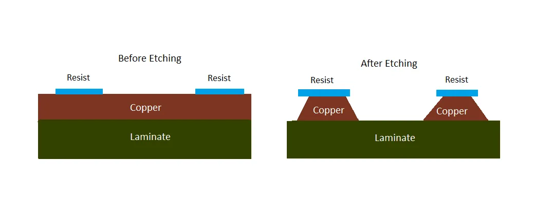
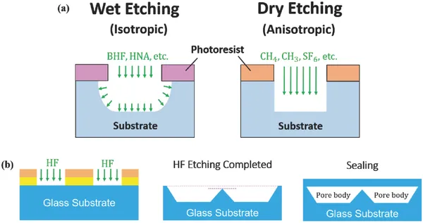
PCB etching relies on chemical or physical mechanisms to dissolve unwanted copper while preserving protected traces under photoresist or seed layers. In wet etching, common for subtractive processes, etchants like ferric chloride attack exposed copper isotropically, creating slight undercuts and trapezoidal profiles. This suits coarser features but limits fine line PCB etching due to lateral etching rates exceeding vertical ones. Dry etching, conversely, employs plasma or reactive ions for anisotropic removal, directing bombardment downward for straighter sidewalls. Factories balance etch factor, temperature, and conveyor speed to control uniformity across panels. These principles scale to HDI through integration with laser direct imaging for pattern definition.
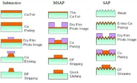
Subtractive etching starts with copper foil laminated to dielectric, coated with dry film resist, exposed, and developed before immersion in etchant. For HDI layers, thinner copper foils, around 1 oz or less, minimize etch time and damage. Additive processes flip this by seeding thin copper on dielectrics, plating traces, and flash-etching excess, ideal for micro etching PCB features. Plasma etching uses ionized gases like carbon tetrafluoride and oxygen in vacuum chambers, enhancing directionality via ion density control. Temperature and pressure adjustments accelerate rates while preserving corners. Understanding these mechanisms allows engineers to select processes matching design rules.
Advanced Etching Techniques for Fine Line and High-Resolution PCBs
Advanced etching techniques elevate HDI PCB etching beyond standard subtractive methods, targeting lines under 50 microns with vertical sidewalls. The semi-additive process (SAP) deposits a 0.1 to 1 micron electroless copper seed, applies resist, electroplates traces to full thickness, strips resist, and flash-etches the seed layer. This yields smooth transitions and suits rigid-flex HDI boards. Modified SAP (mSAP) refines this with ultra-thin base copper, reducing etch exposure for tolerances as tight as ±0.1 mil, crucial for high-resolution PCB routing. Factories use mSAP for UHDI prototypes in wearables and implants, blending with sequential lamination to cut cycles.
Laser direct imaging (LDI) complements these by projecting patterns without films, achieving sub-4 mil registration for fine line PCB etching. Paired with thick resists, LDI prevents defects in dense BGA fanouts. Reactive ion etching (RIE), a dry method, bombards surfaces in plasma for micro-fabrication, minimizing horizontal etch and enabling 20-micron medical traces. Plasma desmear preprocesses vias before plating, removing resin smear for reliable fills. For embedded traces, plasma patterns dielectrics before metallization, shielding from etchants. These techniques, per IPC-6016 qualification specs, ensure HDI layers withstand thermal cycling.
Micro etching PCB demands hybrid approaches in sequential build-up: laser-drill microvias, fill or cap, image outer layers with LDI, and etch using mSAP chemistry. Stacked vias benefit from controlled etch to avoid notching near pads. Factories monitor etch profiles via cross-sections, targeting rectangularity over trapezoids. Advanced etchants optimize rates for low-loss dielectrics with Dk values of 2.8 to 3.5.
Best Practices for Implementing Advanced Etching in HDI Production
Start with design rules aligned to fab capabilities: minimum 2-3 mil line/space, microvia aspect ratios under 0.8:1, and staggered stacking to limit layers. Select low-CTE materials matching copper to prevent delamination post-etch. In factories, preheat panels and conveyorize etching for uniformity, adjusting spray pressure to counter anisotropy. For SAP/mSAP, validate seed adhesion via peel tests before plating. IPC-6012E outlines performance for rigid boards, guiding etch strip and clean steps.
Optimize resist thickness for fine features, using tenting to protect vias during etch. Post-etch, inspect for undercuts with automated optical systems, targeting zero-width reduction. Collaborate on stackups early, placing power/ground planes near surfaces for impedance control. Avoid acute trace angles to prevent chemistry traps. Thermal vias and simulations aid heat dissipation in dense etches. Cleanroom handling preserves ultra-fine traces during lamination.
Challenges in HDI PCB Etching and Troubleshooting Strategies
Fine line PCB etching faces undercutting in subtractive processes, widening spaces beyond tolerances. Solution: Shift to mSAP for minimal lateral etch. Sidewall roughness from isotropic wet methods degrades signals; plasma etching rectifies with directional ions. Overetching in dense areas stems from etchant depletion; factories use high-flow sprays and monitoring. Microvia smear post-drill requires plasma desmear before plating and etch.
Lamination warpage shifts alignments, impacting subsequent etches; thin build-up films and symmetric stacks mitigate. Yield drops below 35 microns demand LDI and cleanrooms. Troubleshoot via cross-sections and etch factor calculations. Per IPC-6016, qualify HDI for reliability under reflow.
Conclusion
Advanced etching techniques like mSAP, LDI, and plasma etching define the frontier of HDI PCB etching, enabling high-resolution PCBs with unprecedented density. Factory insights emphasize process control, material synergy, and standards compliance for robust outcomes. Engineers gain from hybrid subtractive-additive flows in sequential build-ups, balancing cost and performance. As demands for finer features intensify, these methods ensure signal integrity and miniaturization. Adopting best practices positions designs for high yields and innovation.
FAQs
Q1: What distinguishes fine line PCB etching in HDI boards from standard processes?
A1: Fine line PCB etching for HDI targets lines under 50 microns using mSAP or plasma to achieve vertical sidewalls, unlike subtractive wet etching's trapezoidal profiles. Factories control seed layers and etch times to prevent undercuts, aligning with IPC-2226 design rules. This supports microvias and via-in-pad for dense routing. Reliability improves with LDI patterning.
Q2: How does plasma etching enhance advanced etching techniques for high-resolution PCBs?
A2: Plasma etching provides anisotropic removal via ion bombardment, ideal for micro etching PCB features under 25 microns. It minimizes lateral etch for clean corners and integrates with desmear for vias. Production uses controlled gases and vacuum for uniformity. Challenges like plasma uniformity resolve through parameter tuning.
Q3: What are key best practices for HDI PCB etching in sequential build-up?
A3: Prioritize thin copper foils, LDI imaging, and mSAP for fine line precision in HDI PCB etching. Stagger microvias, match CTEs, and inspect post-etch per IPC-6016. Symmetric stackups prevent warpage. Early fab collaboration optimizes tolerances.
Q4: Why is LDI critical for advanced etching techniques in HDI manufacturing?
A4: LDI enables maskless, high-precision patterning for fine line PCB etching below 4 mils, reducing alignment errors in HDI layers. It suits dense BGA escapes and sequential lamination. Factories pair it with thick resists for defect-free etches.
References
IPC-2226 — Sectional Design Standard for High Density Interconnect (HDI) Printed Boards. IPC
IPC-6016 — Qualification and Performance Specification for High Density Interconnect (HDI) Layers or Boards. IPC
IPC-6012E — Qualification and Performance Specification for Rigid Printed Boards. IPC, 2017