Introduction
Blind and buried vias represent critical interconnects in high-density interconnect (HDI) printed circuit boards, enabling compact designs with superior routing density. These vias differ from traditional through-hole vias by connecting only specific layers, which reduces board size and improves signal integrity in advanced electronics. However, their implementation introduces unique challenges related to via reliability, particularly under thermal cycling, mechanical stress, and high-frequency operations. Advanced PCB materials play a pivotal role in mitigating these issues, offering enhanced thermal stability, low dielectric loss, and robust plating adhesion. High-frequency laminates, thermal management materials, and specialized plating materials are at the forefront of these advancements, directly impacting HDI PCB materials performance. Selecting the right combination ensures longer service life and consistent electrical performance in demanding applications like telecommunications and automotive electronics.
Engineers designing for electric systems must prioritize via reliability to prevent failures such as cracking or delamination during assembly or operation. Materials with matched coefficients of thermal expansion (CTE) minimize stress at via interfaces, while low-loss dielectrics preserve signal quality. This article explores how these PCB materials enhance blind and buried via performance, drawing on engineering principles and manufacturing insights. By understanding material properties and selection criteria, designers can achieve reliable HDI structures that meet rigorous performance demands.
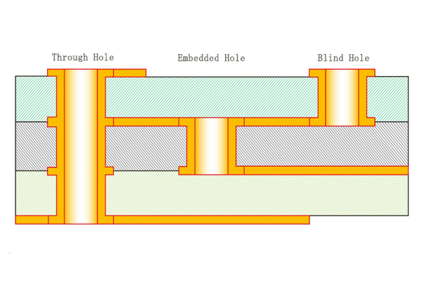
Understanding Blind and Buried Vias and Their Importance
Blind vias connect an outer layer to an immediate inner layer without penetrating the entire board stackup, while buried vias link two or more inner layers exclusively. This configuration allows for finer pitch routing and more layers in HDI PCB materials, essential for miniaturization in modern devices. In high-speed applications, these vias reduce stub lengths, minimizing signal reflections and electromagnetic interference compared to full through-vias. Their relevance grows in sectors requiring high via reliability, such as 5G infrastructure and high-performance computing, where board real estate is at a premium.
The shift toward blind and buried vias stems from the need to pack more functionality into smaller footprints without compromising electrical performance. However, their partial depth exposes them to unique failure modes, including voiding in plating and resin shrinkage during lamination. Proper PCB materials selection addresses these by providing uniform dielectric properties and adhesion strength across layers. Engineers benefit from this approach by achieving higher interconnect density while maintaining signal integrity up to multi-GHz frequencies.
Challenges in Via Reliability for Blind and Buried Structures
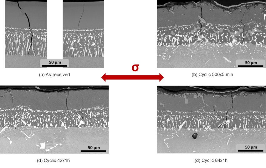
Blind and buried vias face intensified reliability challenges due to sequential lamination processes, which can induce warpage and via barrel stress. Thermal mismatch between copper plating and laminate resins leads to cracking under coefficient of thermal expansion differences during reflow soldering or operational heating. In high-frequency environments, dielectric losses from standard FR-4 materials degrade signals, necessitating advanced PCB materials like high-frequency laminates with low dissipation factors. Additionally, plating integrity is compromised by electroless copper's tendency to thin at via bottoms, risking open circuits.
Mechanical stresses from drilling and plating further exacerbate issues, as microvias in blind structures are prone to nail-heading or flare-out. Environmental factors, such as humidity absorption, cause swelling that stresses via interfaces, leading to delamination. IPC-6012E outlines qualification requirements for rigid printed boards, emphasizing via pull strength and thermal cycle testing to ensure robustness. Addressing these demands via reliability through material innovations is crucial for electric engineers targeting long-term field performance.
Advanced PCB Materials: High-Frequency Laminates
High-frequency laminates serve as the backbone for blind and buried vias in RF and microwave applications, featuring low dielectric constant (Dk) and dissipation factor (Df) values below 3.5 and 0.005, respectively. These materials, often reinforced with low-CTE glass fabrics, reduce signal propagation delays and attenuation, critical for HDI PCB materials in high-speed designs. Their high glass transition temperature (Tg) above 170°C prevents softening during multiple lamination cycles required for buried vias. Uniform resin flow during pressing ensures complete via fill without voids, enhancing mechanical integrity.
Compared to standard epoxies, high-frequency laminates exhibit superior dimensional stability, minimizing via misalignment in stacked structures. Engineers specify these for via reliability in environments with frequencies exceeding 10 GHz, where phase shifts must remain under 1 degree per inch. Thermal stability also aids blind via formation, as low z-axis CTE matches copper's expansion, reducing shear stress. Practical integration involves sequential build-up processes, where each lamination layer uses compatible prepregs to maintain stackup uniformity.
Thermal Management Materials for Via Stress Reduction
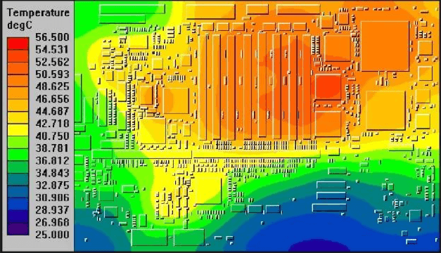
Thermal management materials incorporate fillers like ceramics or metal oxides to achieve thermal conductivity exceeding 1 W/mK, far surpassing conventional laminates. These dissipate heat from densely packed vias, preventing hotspots that accelerate plating fatigue in buried structures. In HDI designs, blind vias act as thermal paths, and high-conductivity cores distribute loads evenly across layers. This approach enhances via reliability by limiting temperature gradients that cause CTE-induced failures.
Hybrid thermal laminates combine low Dk with conductivity, ideal for mixed-signal boards with blind vias carrying high-power signals. During manufacturing, these materials resist drill smear due to tougher resins, simplifying desmear processes before plating. Engineers leverage them in automotive and aerospace applications, where vias endure -40°C to 125°C cycles. IPC-A-600K provides acceptability criteria for such boards, focusing on void-free vias and smooth plating.
Plating Materials and Via Fill Techniques
Plating materials, primarily electroless copper followed by electroplated copper, form the conductive barrel in blind and buried vias, requiring thicknesses of 18-35 μm for current carrying. Advanced formulations include pulse plating to achieve uniform deposition in high-aspect-ratio vias, preventing dog-boning effects. Alloyed coppers with palladium activators improve adhesion to laminate surfaces, crucial for reliability under flexing. Filled via processes use conductive pastes or electroplating to solidly fill blind vias, eliminating air gaps that trap moisture.
For HDI PCB materials, direct metallization skips electroless steps, enabling finer vias with better step coverage. These plating materials enhance thermal cycling endurance by reducing brittleness at via corners. JEDEC J-STD-020E classifies moisture sensitivity, guiding bake-out before plating to avoid popcorn cracking. Engineers select plating based on via diameter-to-depth ratios, typically under 1:1 for blind structures, ensuring plating current reaches bottoms effectively.
Best Practices for Material Selection and Integration
Selecting PCB materials begins with analyzing stackup requirements, matching laminate CTE to copper (17 ppm/°C) across z-axis for via reliability. Simulation tools model thermal-mechanical stresses, guiding choices between high-frequency laminates and thermal variants. Prototype testing verifies via integrity via cross-sectioning and thermal shock per industry protocols. Factory processes emphasize controlled lamination pressures to avoid resin starvation around buried vias.
Layer sequencing optimizes blind via placement, grouping them to minimize lamination counts. Prepreg selection ensures flow compatibility, preventing bridging between fine-pitch vias. Quality checks include electrical continuity and thermal cycle simulations to 1000 cycles. Integrating these practices yields HDI boards with via yields exceeding 99%.
Reliability Testing and Validation Methods
Engineers validate via reliability through accelerated life testing, including temperature cycling from -55°C to 125°C and high-temperature storage. Microvia integrity checks use scanning electron microscopy to detect plating cracks post-test. Warpage measurements ensure stackups stay under 0.75% per IPC guidelines. These methods confirm that advanced PCB materials sustain performance in real-world vibrations and humidity.
Dye-and-peel tests reveal delamination risks at via sites, while thermal impedance mapping quantifies heat paths. Combining high-frequency laminates with robust plating ensures low insertion loss under bias stress.
Conclusion
Advanced PCB materials fundamentally elevate blind and buried via performance in HDI designs, addressing thermal, mechanical, and electrical challenges head-on. High-frequency laminates preserve signal fidelity, thermal management materials control stresses, and optimized plating ensures durable interconnects. Via reliability hinges on precise material matching and process control, enabling compact, high-performance boards for electric engineering applications. By adhering to standards like IPC-6012E and IPC-A-600K, designers achieve robust solutions that withstand operational rigors. Future trends point toward even lower-loss materials, further pushing density limits while maintaining reliability.
FAQs
Q1: What role do high-frequency laminates play in via reliability for HDI PCBs?
A1: High-frequency laminates with low Dk and Df minimize signal loss in blind and buried vias, essential for GHz operations. Their high Tg and low CTE reduce cracking during thermal cycles, enhancing overall via reliability. Sequential lamination compatibility ensures uniform stackups without voids. Electric engineers select them for telecom boards to meet stringent performance specs.
Q2: How do thermal management materials improve blind via performance?
A2: Thermal management materials boost heat dissipation around blind vias, limiting temperature rises that stress plating. High conductivity fillers match CTE, preventing delamination in multilayer HDI PCB materials. They support dense routing by evenly distributing thermal loads. Testing per JEDEC J-STD-020E validates endurance under reflow. This is key for power-intensive electric designs.
Q3: Why are plating materials critical for buried via reliability?
A3: Plating materials like uniform electroplated copper provide robust barrels resistant to fatigue in buried vias. Pulse techniques ensure bottom coverage in high-aspect ratios, avoiding opens. Adhesion promoters enhance laminate bonding, vital for mechanical stress. IPC-A-600K criteria guide acceptability for production. Engineers prioritize them for long-term HDI reliability.
Q4: What factors influence PCB materials selection for via reliability?
A4: CTE matching, Tg, and conductivity dictate PCB materials choices for blind and buried vias. High-frequency needs favor low-loss laminates, while power demands require thermal variants. Manufacturing yield considers drillability and plating compatibility. Standards like IPC-6012E ensure qualification. Balanced selection optimizes HDI performance.
References
IPC-6012E - Qualification and Performance Specification for Rigid Printed Boards. IPC, 2017
IPC-A-600K - Acceptability of Printed Boards. IPC, 2020
JEDEC J-STD-020E - Moisture/Reflow Sensitivity Classification. JEDEC, 2014


