Introduction
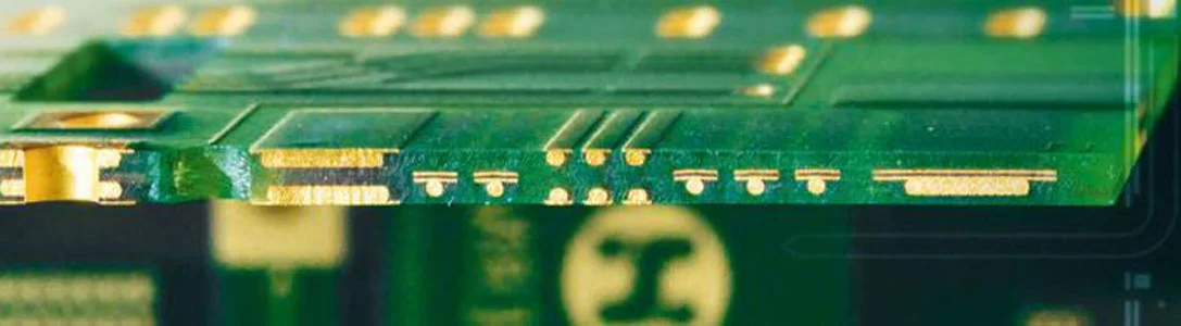
Aerospace applications demand printed circuit boards that operate flawlessly under severe conditions, including rapid temperature swings, high vibration, and substantial mechanical loads. Thick copper PCBs emerge as a cornerstone in high-reliability PCB design, providing the robustness needed for mission-critical systems like avionics, radar, and satellite electronics. Unlike standard PCBs with thin copper layers around 1 oz per square foot, thick copper variants feature layers exceeding 3 oz, often up to 10 oz or more, to handle elevated currents and dissipate heat effectively. This construction enhances overall board integrity, reducing failure risks in extreme environments. Engineers specifying aerospace PCB materials must prioritize thick copper to ensure long-term performance amid thermal cycling and structural stresses.
Understanding Thick Copper PCBs in Aerospace Contexts
Thick copper PCBs for aerospace integrate heavier copper foils during lamination, creating traces and planes with greater cross-sectional area for superior current density and thermal conductivity. In avionics where power demands spike during maneuvers or engine starts, these boards prevent hotspots that could degrade components or cause delamination. The increased copper thickness also bolsters mechanical strength, countering warpage from coefficient of thermal expansion mismatches between copper and dielectrics. Manufacturing processes for such boards involve sequential lamination to manage the challenges of etching thick copper uniformly without undercuts or over-etching. High-reliability PCB design thus relies on this approach to meet the stringent uptime requirements of flight systems.
Aerospace PCB materials selection pairs thick copper with laminates exhibiting low moisture absorption and high glass transition temperatures to withstand -55°C to over 125°C excursions. The copper's ductility absorbs cyclic stresses better than thinner layers, minimizing microcracks in plated through-holes under vibration. Fabricators control plating thickness in vias to at least 25 microns, often more for heavy copper, ensuring void-free barrels that endure thousands of thermal cycles. This combination defines why thick copper stands out in extreme environment PCB manufacturing.
The Engineering Mechanisms Behind Thick Copper Reliability
Thick copper excels in thermal management by offering lower electrical and thermal resistance, allowing heat from power devices to spread rapidly across the plane. During operation, semiconductors generate joule heating proportional to I squared R losses, and thicker copper slashes R, curbing temperature rises that accelerate electromigration. In multilayer stacks, embedded thick copper cores act as heat spreaders, channeling flux away from sensitive vias and reducing via thermal fatigue. This mechanism proves vital in radar arrays where pulsed high currents demand instantaneous dissipation without board flexure.
Mechanical reliability stems from copper's higher yield strength in thicker forms, resisting tensile stresses from differential expansion during cool-down from lamination or reflow. IPC-6012E outlines performance specs for rigid boards, emphasizing dimensional stability under load, which thick copper inherently supports by stiffening the structure. Vibration in aircraft fuselages induces fatigue in traces; thicker sections dampen resonant amplitudes, extending mean time between failures. These principles underpin high-reliability PCB design for sustained integrity.
Under electromagnetic interference prevalent in cockpits, thick copper planes shield signals better due to skin effect advantages at high frequencies, maintaining signal integrity. Corrosion resistance improves with thicker foils, as pinholes or pits affect a smaller percentage of the conductor. Overall, these mechanisms position thick copper as indispensable for aerospace-grade PCBs.
Challenges in Extreme Environment PCB Manufacturing
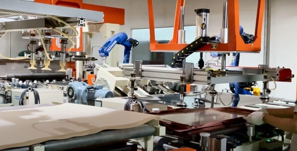
Extreme environment PCB manufacturing for aerospace grapples with the difficulties of handling thick copper foils, which demand specialized presses to achieve uniform bonding without voids. Differential etching rates between copper and resist necessitate slower etchants and precise control to avoid trace widening or necking. Sequential build-up processes layer additional thick copper sheets, mitigating interlaminar stress concentrations that plague all-at-once lamination. Fabricators must validate each step to prevent barrel cracks in vias, a common failure mode under thermal shock.
Material interactions pose risks, as thick copper's expansion coefficient of 17 ppm/°C contrasts with FR-4's 12-16 ppm/°C, potentially cracking dielectrics if not resin-rich. High-reliability PCB design incorporates filled vias or blind structures to isolate stresses, but manufacturing yields drop with copper weights above 6 oz. Cleanliness controls per IPC standards prevent ionic contamination that accelerates dendrite growth under humidity biases seen at altitude. These hurdles underscore the need for process qualification in aerospace PCB materials production.
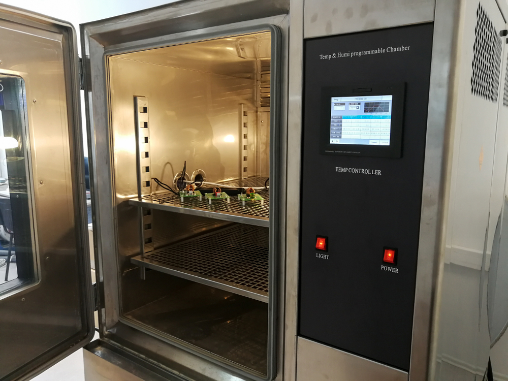
Thick Copper PCB Thermal Stress Testing Essentials
Thick copper PCB thermal stress testing simulates aerospace profiles, cycling boards from cryogenic lows to elevated highs at rates mimicking ascent or re-entry. Air-to-air chambers expose assemblies to 1000+ cycles, monitoring resistance changes and visual defects per IPC-TM-650 methods. Thermal shock via liquid nitrogen immersion reveals latent plating cracks invisible in slower ramps, critical for via reliability. Engineers analyze warpage post-test, as bow and twist exceed 0.75% signal impending delamination.
Vibration overlays thermal loads in combined testing, where accelerometers capture trace strain under 20g peaks. Acoustic microscopy detects subsurface voids exacerbated by copper thickness. High-reliability PCB design validates stack-ups through finite element modeling beforehand, correlating to empirical data. These protocols ensure thick copper withstands the cumulative damage in service.
Best Practices for High-Reliability PCB Design with Thick Copper
Start with stack-up optimization, placing thick copper on inner layers for power distribution while outer layers host fine-pitch signals. Incorporate thermal vias arrays under hotspots, plated to match trace thickness for isothermal flow. Design rules widen traces per current capacity charts, factoring ambient derating for enclosed avionics bays. Simulate CTE-induced stresses using tools compliant with IPC-2221 guidelines to preempt fatigue sites.
Material qualification selects polyimides or high-Tg epoxies for core compatibility with thick copper. Fabrication partners must demonstrate capability via first-article inspections, including cross-sections verifying plating uniformity. Assembly considers heavier boards' handling, using low-stress solders to avoid copper dissolution. Post-assembly, bake-out removes moisture before conformal coating, enhancing humidity resistance.
Field returns analysis refines designs, correlating failures to under-thickened regions. Procurement specs mandate traceability from foil to finished board, aligning with ISO 9001 quality systems. These practices cement thick copper's role in extreme environment PCB manufacturing.
Conclusion
Thick copper PCBs for aerospace deliver unmatched reliability by mastering thermal dissipation, mechanical endurance, and current handling in unforgiving scenarios. High-reliability PCB design leverages this technology to surpass standard boards, ensuring mission success where failure equates to catastrophe. From manufacturing intricacies to rigorous testing, every facet prioritizes longevity under extremes. Engineers gain confidence specifying aerospace PCB materials with thick copper, backed by proven engineering principles and standards adherence. Future advancements will further refine these boards for hypersonic and deep-space ventures.
FAQs
Q1: What makes thick copper PCB for aerospace superior in high-reliability PCB design?
A1: Thick copper layers provide enhanced thermal conductivity and mechanical strength, crucial for handling high currents and vibration in avionics. They reduce via fatigue from CTE mismatches during thermal cycling, extending operational life. Manufacturing focuses on uniform plating to prevent defects, aligning with performance specs for rigid boards. This ensures consistent performance in power-heavy systems like radar.
Q2: How does extreme environment PCB manufacturing adapt for thick copper?
A2: Processes use sequential lamination and specialized etching to manage thick foils, avoiding warpage or undercuts. Laminates with high Tg pair with copper to minimize stress cracks. Qualification verifies void-free bonds and plating thickness, essential for -55°C to 125°C ranges. These steps guarantee durability in aircraft or satellites.
Q3: Why is thick copper PCB thermal stress testing vital for aerospace?
A3: Testing replicates flight cycles, exposing weaknesses in plating or interfaces early. Chambers monitor resistance drift and inspect for microcracks post-1000 cycles. It validates heat spreading efficacy, preventing hotspots in dense layouts. Results guide stack-up tweaks for optimal reliability.
Q4: What aerospace PCB materials complement thick copper best?
A4: High-Tg FR-4 variants or polyimides offer CTE harmony and low moisture uptake, suiting multilayer thick copper builds. These resist delamination under thermal shock while supporting dense vias. Selection per quality systems ensures compatibility for long-term vibration exposure.
References
IPC-6012E — Qualification and Performance Specification for Rigid Printed Boards. IPC, 2015
IPC-TM-650 — Test Methods Manual. IPC, 2020
IPC-A-600K — Acceptability of Printed Boards. IPC, 2020
ISO 9001:2015 — Quality Management Systems. ISO, 2015


