Introduction
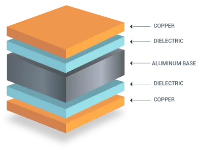
Aluminum printed circuit boards, also known as metal core PCBs, play a critical role in applications requiring superior thermal management, such as power electronics, LED lighting, and automotive systems. These boards feature an aluminum core that efficiently dissipates heat, but their multilayer structure introduces unique manufacturing challenges. Defects during production can compromise electrical performance, mechanical integrity, and long-term reliability. Common issues like aluminum PCB delamination, etching problems, and solder mask defects often stem from material interactions and process variations. Understanding these defects is essential for electric engineers to ensure robust designs and select reliable manufacturing partners. This article explores identification methods, root causes, and preventive strategies aligned with industry best practices.
The Aluminum PCB Manufacturing Process and Why Defects Matter
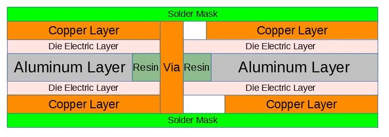
The aluminum PCB manufacturing process begins with preparing the aluminum base plate, typically coated with a thin dielectric layer for insulation, followed by copper foil lamination under controlled heat and pressure. Subsequent steps include dry film imaging, chemical etching to form circuits, application of solder mask, and final routing and testing. Unlike standard FR-4 boards, the coefficient of thermal expansion mismatch between aluminum, dielectric, and copper heightens defect risks during these stages. Defects not only lead to yield losses but also cause field failures, increasing costs and delaying production. For electric engineers, mastering aluminum PCB quality control ensures compliance with performance demands in high-reliability sectors. Early defect prevention maintains signal integrity and thermal performance throughout the product lifecycle.
Aluminum PCB Delamination: Causes and Identification
Aluminum PCB delamination occurs when layers separate, often between the copper foil and dielectric or the dielectric and aluminum core, visibly appearing as blisters, bubbles, or lifting edges under inspection. This defect arises primarily from moisture absorption in the dielectric prepreg, leading to steam generation during lamination or reflow. Contamination on the aluminum surface, such as oils or oxides, weakens adhesion, while excessive lamination pressure exacerbates thermal stresses due to material expansion differences. Engineers can identify it through cross-section microscopy or ultrasonic scanning, which reveals voids or separations. In severe cases, delamination propagates under thermal cycling, compromising board integrity. Adhering to IPC-6012E qualification specs helps classify acceptable bond strength.
Thermal mismatch compounds the issue, as aluminum expands more than the dielectric during heating, inducing shear forces at interfaces. Poor prepreg flow during lamination traps air pockets, creating weak bonds prone to failure. Factory inspections using peel strength tests per IPC-A-600 acceptability criteria detect early signs before full production. Delamination not only affects electrical isolation but also accelerates corrosion in humid environments. Proactive surface preparation remains key to mitigating these risks in the aluminum PCB manufacturing process.
Aluminum PCB Etching Problems: Identification and Root Causes
Etching problems in aluminum PCBs manifest as under-etching, leaving residual copper bridges, or over-etching, causing line width narrowing and trace thinning. These issues disrupt circuit patterns, leading to shorts or opens that fail electrical testing. Uneven etch rates often result from inconsistent developer chemistry, spray pressure variations, or photoresist adhesion failures during the imaging step. The aluminum base requires masking to prevent base metal attack, and any pinholes in the resist amplify defects. Visual inspection under magnification or automated optical inspection reveals sidewall undercutting, where etchant laterally attacks copper beneath the resist. Optimizing etch parameters prevents these flaws from propagating to assembly.
In the aluminum PCB manufacturing process, copper thickness variations post-lamination contribute to etching inconsistencies, as thicker areas etch slower. Agitation inadequacies in the etch tank cause localized depletion of active chemicals, worsening uniformity. Engineers identify problems via dimension metrology, comparing etched traces to design tolerances. Such defects increase impedance variations, critical for high-frequency applications. Maintaining etch factor ratios through process controls ensures predictable outcomes.
Aluminum PCB Solder Mask Issues: Detection and Prevention Strategies
Solder mask issues on aluminum PCBs include peeling, blistering, or incomplete coverage, often appearing as white spots, bubbles, or exposed copper after curing. Poor adhesion stems from surface contamination post-etching, such as residual etchants or oxides not fully neutralized. Thermal shock during mask application or curing causes bubbling, as trapped solvents vaporize. Liquid photoimageable (LPI) masks demand precise exposure and development to avoid pinholes that expose traces to corrosion. Crosshatch adhesion tests per industry norms verify mask integrity before shipping. These defects heighten risks of solder wicking or bridging during assembly.
Curing profiles mismatched to the aluminum substrate's thermal conductivity lead to uneven hardening, promoting cracks under flexure. Factory-driven quality checks, including tape tests, quickly flag weak masks. In high-density designs, mask misalignment with pads compromises solder joint reliability. Addressing these through plasma cleaning enhances wetting and durability. Aluminum PCB solder mask issues directly impact environmental protection and conformal coating compatibility.
Comprehensive Aluminum PCB Quality Control Measures
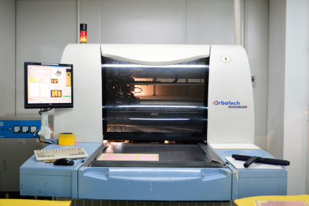
Effective aluminum PCB quality control integrates in-process monitoring and final validation to catch defects early. Incoming inspection of aluminum sheets verifies flatness and oxide-free surfaces, while lamination presses log temperature, pressure, and vacuum levels for traceability. Post-etching, electrical continuity tests detect opens or shorts from etching problems. Thermal shock and thermal cycling per IPC standards simulate end-use stresses, revealing latent delamination. Warpage measurement using shadow moiré ensures bow and twist stay within limits, vital for automated assembly. Statistical process control charts track key variables like etch uniformity across panels.
Visual and X-ray inspections complement automated systems for void detection in dielectrics. Solder mask thickness gauging prevents issues like outgassing during reflow. Implementing ISO 9001:2015 quality management systems standardizes these protocols, fostering continuous improvement. For electric engineers, specifying Class 2 or 3 per IPC-A-600 aligns with reliability needs. This multilayered approach minimizes scrap and elevates yield rates.
Best Practices for Prevention and Solutions
Preventing defects starts with design for manufacturability, specifying dielectric materials with matched CTE to aluminum and adequate peel strength. Pre-lamination baking at controlled conditions removes moisture, a primary delamination culprit. Surface treatment via chemical etching or anodizing enhances aluminum wettability before dielectric application. For etching, maintaining consistent ferric chloride or cupric solutions with agitation controls undercutting. Solder mask application benefits from pre-bake cleaning and optimized UV exposure to ensure uniform thickness.
Process validation through capability studies refines parameters, reducing variations. Supplier qualification ensures consistent prepreg and copper foil quality. Rework for minor defects involves localized stripping and reapplication, but prevention trumps repair. Training operators on IPC guidelines builds competency. These factory-driven practices yield defect-free aluminum PCBs ready for demanding applications.
Troubleshooting Real-World Scenarios
In one scenario, persistent delamination traced to inconsistent lamination dwell time was resolved by standardizing press cycles, improving yield by stabilizing bond formation. Etching undercuts in fine-pitch traces often link to aged chemistry; regular solution analysis and replenishment restored line fidelity. Solder mask blisters post-cure pointed to overexposure, corrected via dosimetry calibration for even energy distribution. Warpage exceeding specs from asymmetric layer buildup demanded balanced stacking sequences. These insights underscore iterative process tuning guided by data logs.
Conclusion
Aluminum PCB manufacturing defects like delamination, etching problems, and solder mask issues pose significant hurdles but are manageable through rigorous quality control and process optimization. Electric engineers benefit from specifying standards-compliant boards to safeguard performance. By prioritizing surface preparation, precise parameter control, and inline inspections, manufacturers deliver reliable products. Embracing these strategies minimizes risks across the aluminum PCB manufacturing process, ensuring thermal and electrical excellence in final assemblies.
FAQs
Q1: What causes aluminum PCB delamination and how can it be prevented?
A1: Aluminum PCB delamination typically results from moisture in the dielectric, contamination, or thermal expansion mismatches during lamination. Prevention involves baking panels to remove absorbed water, thorough surface cleaning of the aluminum core, and controlled lamination parameters for optimal flow and bonding. Adhering to IPC-6012E specs ensures verified interlayer adhesion. Regular peel tests during quality control catch potential issues early.
Q2: How do you identify and fix aluminum PCB etching problems?
A2: Aluminum PCB etching problems appear as undercuts, over-etching, or residue via visual or AOI inspection, often due to inconsistent chemistry or resist adhesion. Solutions include monitoring etch rates, improving agitation, and refreshing solutions regularly. Dimension verification post-etch confirms tolerances. Process adjustments prevent recurrence in production runs.
Q3: What are common aluminum PCB solder mask issues and prevention tips?
A3: Common issues include peeling, blisters, or pinholes from poor adhesion or curing defects. Prevent by plasma cleaning post-etch, optimizing exposure times, and adhesion testing. Uniform thickness gauging supports quality control. These steps enhance protection against environmental factors.
Q4: Why is aluminum PCB quality control critical in manufacturing?
A4: Aluminum PCB quality control detects defects like warpage or voids early, ensuring reliability in thermal-intensive apps. It involves IPC-aligned inspections, from material incoming to final electrical tests. Consistent protocols reduce scrap and support scalable production.
References
IPC-6012E — Qualification and Performance Specification for Rigid Printed Boards. IPC, 2017
IPC-A-600K — Acceptability of Printed Boards. IPC, 2020
ISO 9001:2015 — Quality Management Systems. ISO, 2015