Introduction
Aluminum printed circuit boards, also known as metal core PCBs, excel in applications requiring superior heat dissipation, such as power electronics, LED lighting, and automotive systems. These boards feature a thermally conductive aluminum core sandwiched between copper circuit layers and a thin dielectric, enabling efficient heat spreading compared to standard FR-4 substrates. Thermal vias play a critical role in this architecture by providing vertical conduction paths that channel heat from surface-mounted components directly to the aluminum core. Proper implementation of aluminum PCB thermal vias significantly lowers PCB thermal resistance, preventing hotspots and extending component lifespan. Engineers designing high-power density boards must prioritize thermal via design rules to optimize performance without compromising manufacturability. This article explores aluminum PCB thermal via size, placement strategies, and best practices aligned with industry standards for improving thermal performance PCB.
What Are Aluminum PCB Thermal Vias and Why They Matter
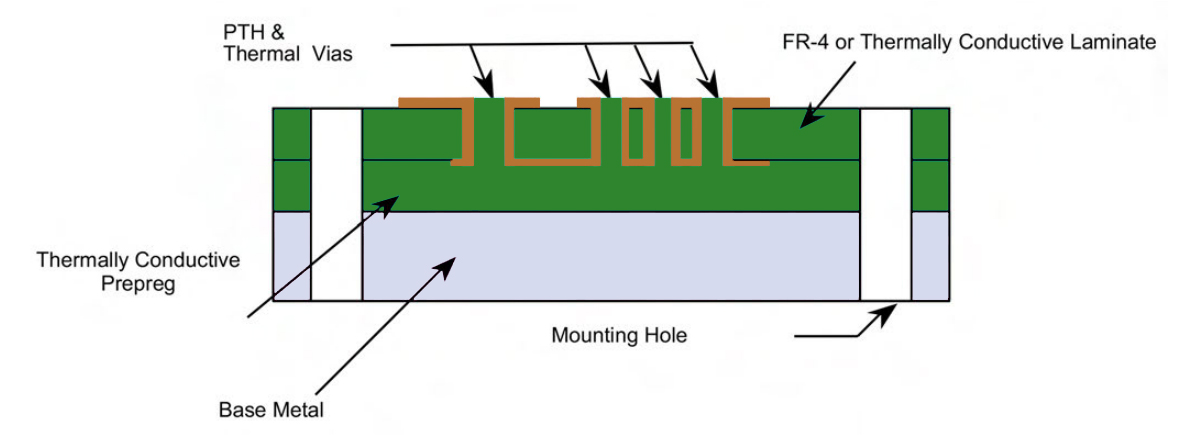
Aluminum PCB thermal vias are plated through-holes strategically placed to transfer heat from the top copper layer through the insulating dielectric to the high-conductivity aluminum base. Unlike signal vias, these prioritize thermal conductivity over electrical isolation, often featuring copper plating or conductive fills to minimize thermal impedance. In metal core constructions, the vias bridge the gap between heat-generating components and the core, which has a thermal conductivity around 200 times higher than FR-4 materials. This setup reduces overall PCB thermal resistance by creating parallel low-impedance heat paths. Without thermal vias, heat remains trapped near the component, leading to elevated junction temperatures, reduced efficiency, and potential failure in demanding environments. Adopting thermal via design rules ensures reliable operation in power converters and high-brightness LEDs, where improving thermal performance PCB is essential.
The relevance extends to modern designs facing increasing power densities, where standard copper planes alone cannot suffice. Thermal vias enable compact layouts by leveraging the aluminum core as a natural heatsink. Designers must consider via integration early to avoid layout conflicts and ensure compliance with fabrication capabilities.
Technical Principles of Thermal Vias in Aluminum PCBs
Heat transfer in thermal vias follows conduction principles, governed by Fourier’s law, where flux is proportional to the temperature gradient and material conductivity. The copper barrel plating, with its high thermal conductivity of approximately 385 W/m·K, forms the primary path, far outperforming the dielectric’s low conductivity. Thermal resistance of a single via is inversely proportional to its cross-sectional area and conductivity, while directly proportional to length, highlighting the need for optimized geometries. In aluminum PCBs, vias terminate at the core, minimizing path length and enhancing effectiveness. Arrays of vias operate in parallel, collectively reducing equivalent thermal resistance and distributing heat evenly to prevent localized stress.
Dielectric thickness, typically 75 to 150 microns in aluminum boards, influences via length and plating uniformity. Poor plating can introduce voids, increasing resistance, so aspect ratios below 10:1 are recommended for reliable electrodeposition. The aluminum core then spreads heat laterally, aided by its high conductivity, before dissipating to ambient or attached heatsinks. Simulations reveal that unfilled vias already outperform substrate conduction, but enhancements like fills amplify gains.
Aluminum PCB Thermal Via Size: Key Considerations
Aluminum PCB thermal via size directly impacts cross-sectional area and thus heat transfer capacity. Drill diameters typically range from 0.2 mm to 0.4 mm (8 to 16 mil), balancing thermal performance with density constraints. Larger diameters lower resistance per via but limit array density under small thermal pads. Finished hole sizes account for plating buildup, usually 0.075 mm minimum plating thickness. Engineers should verify fabricator capabilities, as microvias under 0.15 mm may require advanced processes not suited for aluminum boards.
Aspect ratio, defined as board thickness to drill diameter, must stay under 10:1 to ensure void-free plating and structural integrity. Oversized vias risk core exposure during lamination, compromising insulation. IPC-2221 provides foundational guidelines for via dimensions in thermal management, emphasizing compatibility with overall board stackup. Iterative sizing via thermal modeling refines choices for specific power levels.
Aluminum PCB Thermal Via Placement: Optimizing Heat Flow
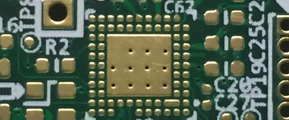
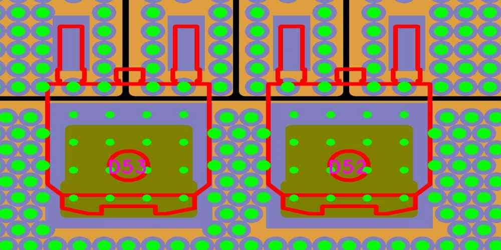
Strategic aluminum PCB thermal via placement maximizes proximity to heat sources while respecting routing needs. Position arrays directly under component thermal pads, such as QFN exposed pads or power transistor bases, to minimize lateral conduction losses. Grid patterns with center-to-center spacing of 1 to 1.2 mm (40 to 48 mil) distribute load evenly without solder wicking risks during assembly. Avoid clustering near board edges or flex zones to prevent warpage.
Connect vias to inner copper planes or directly to the grounded aluminum core for enhanced spreading. In multi-layer aluminum designs, stagger vias across layers to avoid alignment-induced weaknesses. Signal vias should remain separated by at least twice the thermal via diameter to minimize crosstalk. Placement under high-power LEDs, for instance, can reduce hotspot temperatures by channeling heat promptly to the core.
Best Practices for Thermal Via Filling, Density, and Integration
Filling thermal vias with conductive epoxy or copper paste improves performance over plated-only designs by eliminating air gaps and boosting effective conductivity. Capped fills provide flat surfaces for soldering, ideal for dense BGA or QFN footprints. Tenting on the bottom side prevents solder flow, while top exposure aids heat capture. Density guidelines suggest 10 to 50 vias per cm2 under pads, scaled by power dissipation and simulation results.
Integrate vias with wide copper pours and spokes for hybrid conduction. IPC-6012 outlines performance specs ensuring via reliability under thermal cycling. Avoid thermal reliefs on thermal vias, as they impede heat flow. Validate designs with finite element analysis to quantify PCB thermal resistance reductions.
Thicker copper layers (2 oz or more) complement vias by enhancing plane spreading. Ground stitching vias around thermal arrays tie the core to top layers, further lowering impedance. Prototype testing confirms efficacy before production scaling.
Common Challenges and Troubleshooting
Excessive via density can raise fabrication costs and risk dielectric breakdown during core bonding. Symptoms include higher-than-expected temperatures; solutions involve reducing pitch or selective filling. Solder wicking clogs vias, addressed by precise spacing and mask definitions. Warpage from mismatched CTEs appears post-reflow; mitigate with balanced layering per IPC guidelines.
Simulation discrepancies arise from ignoring plating thickness; refine models accordingly. Field failures from via cracking under vibration demand robust annular rings.
Conclusion
Mastering aluminum PCB thermal via design rules unlocks superior thermal management for demanding electronics. Optimal via size, precise placement, and conductive fills collectively slash PCB thermal resistance, enabling reliable high-power operation. Adhering to best practices like grid arrays and plane integration ensures manufacturability and performance. Engineers benefit from early thermal analysis to tailor solutions, aligning with IPC-2152 for current-related thermal predictions. Implementing these strategies elevates design quality, reducing rework and enhancing longevity.
FAQs
Q1: What is the optimal aluminum PCB thermal via size for high-power applications?
A1: Aluminum PCB thermal via size typically ranges from 0.2 mm to 0.4 mm drill diameter to balance heat transfer area with layout density. Larger sizes suit higher dissipation but limit arrays under small pads, while aspect ratios under 10:1 ensure plating quality. Select based on thermal simulations and fabricator specs for best results.
Q2: How does aluminum PCB thermal via placement affect overall thermal performance?
A2: Aluminum PCB thermal via placement under heat sources in grid patterns with 1 mm spacing channels heat efficiently to the core, minimizing hotspots. Proximity to components reduces lateral losses, and connection to ground planes aids spreading. Proper placement per thermal via design rules can significantly improve thermal performance PCB.
Q3: What are key thermal via design rules for reducing PCB thermal resistance?
A3: Thermal via design rules emphasize arrays of 0.3 mm vias spaced 1 mm apart, filled with conductive materials, and integrated with copper planes. Avoid reliefs and maintain low aspect ratios for reliability. These practices lower PCB thermal resistance by providing parallel conduction paths to the aluminum core.
Q4: How can engineers improve thermal performance PCB using thermal vias in aluminum boards?
A4: Engineers improve thermal performance PCB by deploying via arrays under pads, using copper fills, and verifying with simulations. Ground the core and add stitching for even dissipation. Follow IPC standards to ensure durability under cycling.
References
IPC-2221B — Generic Standard on Printed Board Design. IPC, 2003
IPC-2152A — Standard for Determining Current Carrying Capacity in Printed Board Design. IPC, 2009
IPC-6012E — Qualification and Performance Specification for Rigid Printed Boards. IPC, 2018


