Introduction
In the fast-paced world of electronics manufacturing, printed circuit boards (PCBs) serve as the backbone of countless devices. Ensuring their reliability and performance is critical for engineers and manufacturers alike. A key step in achieving this is the PCB cleaning process, which removes contaminants like flux residues, dust, and ionic impurities that can compromise functionality. For electric engineers, understanding automated cleaning processes is vital to maintaining quality in high-volume production. This article explores the importance of the PCB cleaning process for components, the materials used, and best practices to enhance reliability. By addressing contamination risks and leveraging automation, manufacturers can meet stringent industry standards and deliver robust electronic assemblies.
What Is PCB Cleaning and Why It Matters
PCB cleaning refers to the systematic removal of contaminants from the surface of printed circuit boards after soldering or during manufacturing stages. These contaminants include flux residues, solder paste, adhesives, and environmental particles. If left unaddressed, such residues can lead to issues like corrosion, electrical shorts, or signal interference, ultimately reducing the lifespan of electronic devices. For electric engineers, the PCB cleaning process is not just a procedural step but a cornerstone of quality assurance.
The significance of cleaning becomes even more pronounced in high-reliability applications such as aerospace, medical devices, and automotive electronics. In these sectors, even minor defects can result in catastrophic failures. A well-executed cleaning process ensures that components on the PCB maintain proper electrical connectivity and are protected from long-term degradation. As automation becomes prevalent, understanding how to integrate efficient cleaning systems into production lines is essential for consistency and scalability.
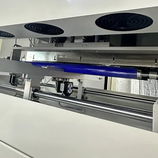
Technical Principles of Automated PCB Cleaning
Automated PCB cleaning operates on the principle of applying controlled cleaning agents, mechanical actions, and drying methods to eliminate contaminants without damaging delicate components. The process typically involves several stages, each tailored to the type of residue and board design.
First, the cleaning medium, often a water-based or solvent-based solution, is selected based on the nature of the contaminants. Water-based solutions are effective for ionic residues, while solvents target organic flux residues. The cleaning agent is applied through methods like spray-under-immersion or ultrasonic agitation. Ultrasonic cleaning, for instance, uses high-frequency sound waves to create cavitation bubbles that dislodge particles from intricate areas of the PCB.
Related Reading: Is Your Ultrasonic Cleaner Damaging Your PCBs? A Guide to Safe Practices
Temperature and pressure are carefully controlled to avoid thermal stress or physical damage to components. After cleaning, rinsing removes any remaining cleaning agent, followed by a drying phase using hot air or vacuum systems to prevent moisture retention. Automation ensures repeatability by standardizing these parameters across large batches, minimizing human error.
Standards like IPC-6012E, which outlines performance specifications for rigid printed boards, emphasize the importance of cleanliness to prevent defects. Adhering to such guidelines during automated cleaning helps engineers achieve consistent outcomes and meet industry expectations for reliability.
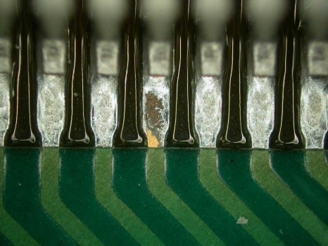
Types of Contaminants and Their Impact on PCBs
Understanding the contaminants targeted by the PCB cleaning process is crucial for electric engineers. Flux residues, commonly left after soldering, are a primary concern. These residues can be rosin-based, water-soluble, or no-clean, each requiring specific cleaning approaches. If not removed, they can attract moisture, leading to corrosion or dendritic growth between conductive traces.
Solder paste residues and metal oxides also pose risks by interfering with electrical contacts. Environmental contaminants like dust or fingerprints introduce ionic impurities that can cause current leakage. In high-frequency applications, even minute residues can disrupt signal integrity, making thorough cleaning indispensable.
Automated systems address these challenges by using precise cleaning cycles tailored to the contaminant type. Engineers must evaluate the PCB design, including component density and spacing, to select the appropriate cleaning method and avoid damage to sensitive parts.
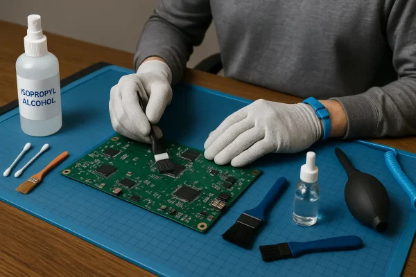
PCB Cleaning Materials and Their Selection
The choice of PCB cleaning materials directly influences the effectiveness of the process. Water-based cleaning agents, often combined with surfactants, are widely used for their ability to dissolve ionic residues. These are preferred in environments where environmental impact is a concern, as they produce less hazardous waste compared to solvents.
Solvent-based materials are effective for removing organic residues like rosin flux. However, their use requires careful handling due to flammability and health risks. Engineers must ensure proper ventilation and compliance with safety standards when integrating solvents into automated systems.
In some cases, specialized cleaning agents are formulated to target specific residues without affecting the PCB substrate or components. The compatibility of cleaning materials with the board materials, such as laminates and solders, must be verified to prevent etching or degradation.
Standards like IPC-CH-65B, which provides guidelines for cleaning electronic assemblies, recommend testing cleaning materials for compatibility before full-scale implementation. This ensures that the selected materials do not introduce new risks during the PCB cleaning process for components.
Best Practices for Automated PCB Cleaning
Implementing an effective automated PCB cleaning process requires adherence to best practices that balance efficiency with reliability. Engineers should start by defining cleaning requirements based on the PCB type and application. For instance, high-density boards with fine-pitch components may require ultrasonic cleaning to reach tight spaces, while simpler designs might suffice with spray cleaning.
Maintaining equipment calibration is essential to ensure consistent application of cleaning agents and drying conditions. Regular inspection of nozzles, filters, and ultrasonic transducers prevents variations that could compromise cleaning quality. Additionally, monitoring the purity of cleaning solutions and rinse water prevents recontamination of boards.
Post-cleaning inspection, guided by standards like IPC-A-600K for acceptability of printed boards, helps verify cleanliness levels. Techniques such as ionic contamination testing can quantify residue levels, ensuring they fall within acceptable limits. Engineers should also document cleaning parameters and outcomes to identify trends or areas for improvement in the process.
Automation software can further enhance efficiency by adjusting cleaning cycles based on real-time feedback from sensors. This adaptability is particularly valuable in high-mix production environments where PCB designs vary frequently.
Related Reading: PCB Cleaning Processes in Mass Production: Ensuring Reliability and Performance
Challenges in Automated PCB Cleaning and Solutions
Despite its advantages, automated PCB cleaning presents challenges that electric engineers must address. One common issue is the risk of component damage due to excessive mechanical force or incompatible cleaning agents. To mitigate this, engineers can conduct pilot tests on sample boards to fine-tune cleaning parameters before scaling up.
Another challenge is managing wastewater and chemical disposal, especially with solvent-based cleaning. Implementing closed-loop systems for recycling cleaning agents reduces waste and ensures compliance with environmental regulations. Regular training for personnel on handling and maintenance of automated systems also minimizes operational errors.
For complex assemblies, shadowing effects can occur, where certain areas of the PCB remain uncleaned due to component placement. Adjusting the orientation of boards during cleaning or using multi-directional spray systems can overcome this limitation. Standards like IPC-J-STD-001H, which covers requirements for soldered electrical and electronic assemblies, provide guidance on achieving uniform cleanliness across intricate designs.
Conclusion
Automated PCB cleaning processes play a pivotal role in ensuring the reliability and performance of electronic assemblies. By systematically removing contaminants, these processes protect components and maintain electrical integrity, which is critical for high-stakes applications. Electric engineers must prioritize the selection of appropriate PCB cleaning materials and adhere to industry standards to achieve consistent results. Through automation, manufacturers can scale cleaning operations while minimizing variability and human error. As technology advances, integrating smart systems and real-time monitoring will further enhance the precision of the PCB cleaning process for components. Ultimately, a commitment to best practices and continuous improvement ensures that PCBs meet the demanding requirements of modern electronics.
FAQs
Q1: What is the importance of the PCB cleaning process in electronics manufacturing?
A1: The PCB cleaning process is crucial for removing contaminants like flux residues and dust that can cause corrosion or electrical failures. By ensuring cleanliness, it enhances reliability and extends the lifespan of electronic devices. Standards like IPC-6012E guide engineers in maintaining quality, making cleaning indispensable for high-performance applications in industries such as aerospace and medical.
Q2: How do PCB cleaning materials impact the cleaning outcome?
A2: PCB cleaning materials, such as water-based or solvent-based agents, directly affect the removal of specific residues. Choosing the right material prevents damage to components and ensures effective cleaning. Compatibility with board materials is vital, as outlined in IPC-CH-65B, to avoid issues like etching or residue recontamination during the process.
Q3: What challenges arise during the PCB cleaning process for components?
A3: The PCB cleaning process for components can face challenges like potential damage from harsh agents or mechanical stress. Shadowing effects in dense assemblies may leave areas uncleaned. Solutions include pilot testing parameters and using multi-directional cleaning systems to ensure uniform results without compromising component integrity.
Q4: How can automation improve the PCB cleaning process?
A4: Automation enhances the PCB cleaning process by standardizing parameters like temperature and pressure, ensuring repeatability across batches. It reduces human error and adapts to varying designs through real-time feedback. This leads to consistent cleanliness levels, critical for meeting standards like IPC-A-600K in high-volume production environments.
References
IPC-6012E — Qualification and Performance Specification for Rigid Printed Boards. IPC, 2020.
IPC-A-600K — Acceptability of Printed Boards. IPC, 2020.
IPC-CH-65B — Guidelines for Cleaning of Printed Boards and Assemblies. IPC, 2011.
IPC-J-STD-001H — Requirements for Soldered Electrical and Electronic Assemblies. IPC, 2021.


