Introduction
In modern PCB manufacturing, achieving high precision and consistency demands advanced imaging techniques. Laser Direct Imaging (LDI) represents a pivotal shift from traditional film-based methods, enabling automated PCB direct imaging directly from digital data. Integrating LDI into your production line streamlines workflows, reduces defects, and supports the demands of high-density interconnects (HDI) and fine-pitch features. This automation aligns with broader PCB manufacturing automation trends, paving the way for smart factory PCB environments where real-time data drives efficiency. Engineers seeking to optimize direct imaging processes must understand LDI's technical foundations and integration strategies to maximize yield and throughput. As production scales, LDI integration emerges as a key enabler for meeting stringent quality requirements in competitive markets.
What Is LDI and Why Does It Matter in PCB Production?
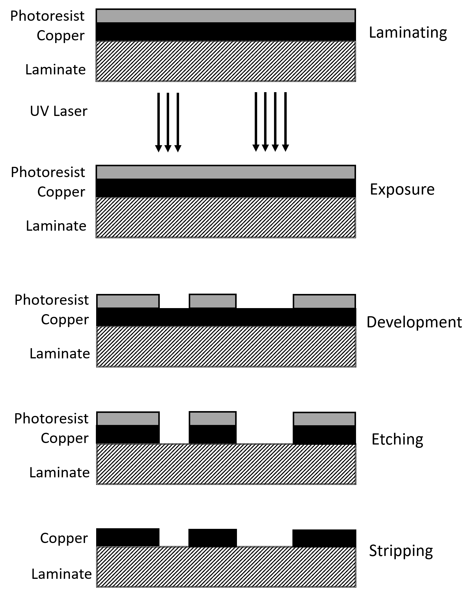
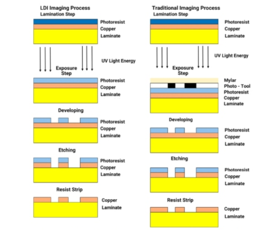
Laser Direct Imaging, or LDI, uses a modulated laser beam to expose photoresist on PCB panels directly from Gerber or ODB++ files, eliminating intermediate photoplots or films. This digital process ensures superior registration accuracy, typically within microns, compared to analog methods prone to shrinkage and alignment errors. In PCB manufacturing, LDI matters because it supports finer line widths and spaces, essential for designs exceeding 50 microns, which conventional imaging struggles to resolve consistently. Automation through LDI integration reduces human intervention, minimizing variability and enabling lights-out operations in smart factory PCB setups. For electric engineers, this means reliable production of multilayer boards with via-in-pad and microvia technologies, directly impacting signal integrity and thermal performance. Ultimately, LDI drives cost savings by cutting material waste and rework, positioning it as a cornerstone of optimizing direct imaging processes.
The relevance extends to compliance with industry benchmarks, where precise imaging prevents defects like over-etching or under-exposure that compromise board reliability. Facilities adopting automated PCB direct imaging report improved first-pass yields, crucial for high-volume runs. Moreover, LDI facilitates rapid prototyping iterations, as changes in design files translate instantly to exposure without film remake delays.
Technical Principles of LDI in Automated Systems
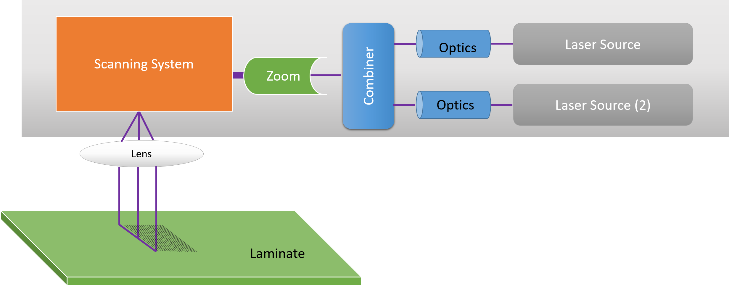
LDI operates on the principle of raster scanning or vector imaging, where a UV laser, often at 355 nm or 405 nm wavelengths, selectively exposes photosensitive dry films or liquid resists. The system's galvo mirrors and projection optics project the digital image onto the panel surface with sub-micron precision, controlled by servo motors and closed-loop feedback. Exposure parameters, including dosage, scan speed, and focus depth, are calibrated to the resist's sensitivity curve, ensuring uniform energy distribution across large panels up to 24x24 inches. In automated setups, software interpolates artwork data, compensating for panel warpage or thickness variations through 3D mapping sensors.
This mechanism outperforms step-and-repeat exposure tools by avoiding stitching errors at panel edges, a common issue in high-resolution imaging. Laser power modulation adapts to resist thickness, preventing overexposure in thinner areas or vias. Integration with metrology tools allows inline verification of critical dimensions (CD), aligning with IPC-6012E specifications for rigid printed boards.
Thermal management plays a role, as continuous operation generates heat that could distort panels; advanced systems incorporate chillers and vacuum hold-downs for stability. Data processing pipelines convert CAM files into exposure paths, optimizing for throughput by prioritizing dense feature areas. These principles enable LDI to handle advanced nodes, supporting the shift toward Industry 4.0 in PCB production.
Integrating LDI into Your Production Line for PCB Manufacturing Automation
Successful LDI integration begins with assessing current workflows, from panel preparation to develop-etch-strip (DES) processes. Position the LDI station post-lamination and resist coating, ensuring cleanroom compatibility to avoid contamination. Interface with upstream MES (Manufacturing Execution Systems) for job queuing, where panels are automatically loaded via robotic handlers onto the imaging table. Calibration routines, run at shift starts, align fiducials using machine vision, achieving overlay tolerances below 10 microns for multilayer imaging.
Software integration is critical; LDI systems must parse extended Gerber formats and support job-specific scaling factors for panel expansion. In smart factory PCB environments, connect LDI to IoT networks for predictive maintenance, monitoring laser diode hours and optics cleanliness. Downtime risks from misalignment can be mitigated by implementing auto-focus algorithms that scan panel topography in real-time.
Hardware choices influence scalability: modular LDI platforms allow throughput scaling from 50 to 200 panels per hour by adding parallel units. Electrical interfaces, such as Ethernet/IP for conveyor synchronization, ensure seamless handoff to developers. Training operators on recipe management optimizes direct imaging processes, with presets for different copper weights and panel sizes.
Best Practices for Optimizing Direct Imaging Processes
To maximize LDI performance, establish rigorous panel preparation protocols, including plasma cleaning to enhance resist adhesion and remove oxides. Optimize exposure dosages through DOE (Design of Experiments), plotting line width versus energy to define process windows. Inline AOI (Automated Optical Inspection) post-imaging verifies feature fidelity before etching, catching anomalies like haloing or bridging early.
Maintenance schedules prevent drift: weekly lens cleaning and quarterly laser alignment sustain resolution. For LDI integration in high-mix environments, develop modular recipes stored in a central database, accessible via barcode scanning. Monitor key metrics like throughput, yield, and CD uniformity using SPC (Statistical Process Control) charts to drive continuous improvement.
Environmental controls are vital; maintain 22-24°C and 45-55% RH to stabilize resist behavior, as per ISO 9001:2015 quality management guidelines. Firmware updates incorporate machine learning for warpage compensation, enhancing registration on bowed panels. Collaborating across engineering teams ensures LDI outputs align with downstream etch and plating capabilities.
Challenges and Troubleshooting in LDI Automation
Common hurdles include ghosting from incomplete resist development or laser scatter on rough copper surfaces. Troubleshoot by adjusting pulse width and verifying vacuum hold-down pressure to flatten panels. Throughput bottlenecks arise in data-heavy designs; optimize by compressing artwork files and using multi-beam lasers.
In multilayer imaging, x-y-z registration errors compound; employ reference marks and fiducial arrays per IPC-A-600K acceptability criteria. Power fluctuations demand UPS backups and diode monitoring to avoid exposure inconsistencies. Scaling to smart factory PCB requires cybersecurity for networked systems, segmenting LDI controls from general IT.
Pilot runs validate integration before full rollout, quantifying improvements in defect rates and cycle times. Vendor-agnostic APIs facilitate future upgrades, ensuring long-term flexibility.
Conclusion
Automating PCB direct imaging through LDI integration transforms production lines into efficient, precise operations aligned with PCB manufacturing automation goals. By mastering technical principles, seamless workflow incorporation, and optimization best practices, engineers unlock higher yields and finer features for demanding applications. Smart factory PCB visions become reality as LDI enables data-driven decisions and reduced variability. Facilities embracing these strategies position themselves for sustained competitiveness, adhering to proven standards for quality and reliability. Invest time in calibration and monitoring to fully realize LDI's potential in your operations.
FAQs
Q1: What are the main benefits of automated PCB direct imaging with LDI?
A1: LDI provides micron-level precision, eliminates film-related defects, and supports high-volume throughput in PCB manufacturing automation. It ensures consistent registration across panels, reducing rework and enabling finer features like 40-micron lines. Integration boosts first-pass yields, aligning with quality standards for reliable boards. This automation scales well for smart factory PCB setups, minimizing operator dependency.
Q2: How does LDI integration improve PCB manufacturing automation?
A2: LDI connects via MES for automated job handling and robotic loading, streamlining from data import to exposure. Real-time feedback loops adjust for panel variations, optimizing direct imaging processes. It reduces cycle times by 30-50% in typical lines while maintaining tolerances. Factory-wide IoT ties LDI data to overall efficiency metrics.
Q3: What steps are involved in optimizing direct imaging processes using LDI?
A3: Start with panel prep and calibration, then fine-tune exposure parameters via testing. Implement inline AOI and SPC for quality control post-imaging. Regular maintenance and environmental controls sustain performance. These practices ensure compliance and high yields in LDI-integrated lines.
Q4: Can LDI handle advanced HDI boards in production?
A4: Yes, LDI excels in HDI with microvias and blind/buried structures, offering superior resolution over film methods. Digital imaging avoids alignment shifts, critical for stacked vias. Process controls per relevant IPC standards verify feature integrity before lamination.
References
IPC-6012E — Qualification and Performance Specification for Rigid Printed Boards. IPC, 2017
IPC-A-600K — Acceptability of Printed Boards. IPC, 2020
ISO 9001:2015 — Quality Management Systems. ISO, 2015


