Introduction
Printed circuit boards have evolved significantly from simple through-hole designs to complex multilayer structures that support modern electronics. Blind and buried vias represent a critical advancement, enabling higher routing density and improved electrical performance in dense interconnects. These vias address limitations of traditional through-holes, which penetrate the entire board and consume valuable surface space. In high-speed PCB design and RF PCB design, blind and buried vias minimize signal discontinuities and parasitics, making them essential for applications demanding precision. This article explores PCB blind via applications and PCB buried via applications, providing engineers with structured insights into their implementation. By understanding these technologies, designers can optimize board performance while adhering to manufacturing constraints.
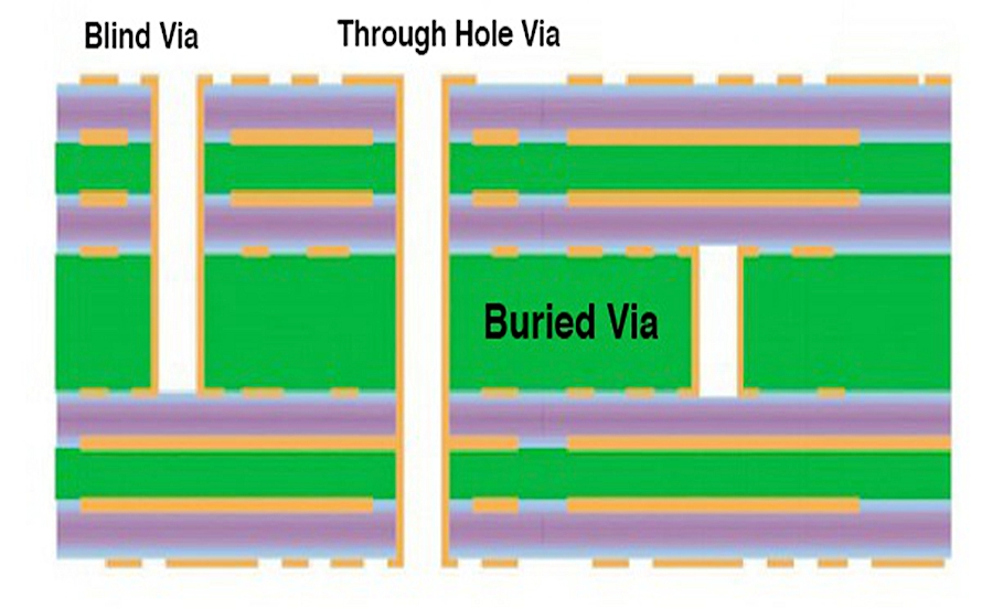
Understanding Blind and Buried Vias
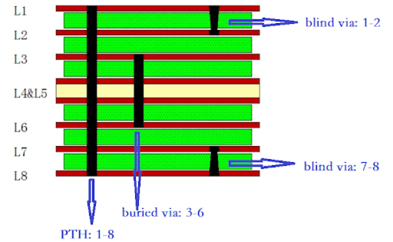
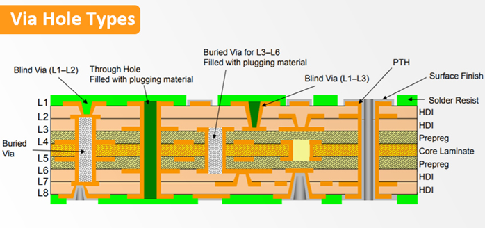
Blind vias connect an outer layer to one or more inner layers without extending through the entire board thickness. Buried vias, in contrast, interconnect only internal layers and remain completely hidden from the external surfaces. Both types are fabricated using sequential lamination processes, where specific layers are drilled and plated before final assembly. This approach allows for finer pitch routing compared to through-holes, which create stubs that degrade high-frequency signals. IPC-2221B outlines design guidelines for minimum drilled hole sizes in blind and buried vias, ensuring manufacturability across layer counts. These vias are particularly relevant in boards exceeding eight layers, where space efficiency drives overall layout success.
The distinction between blind and buried vias lies in their accessibility during fabrication. Blind vias require controlled depth drilling, often with laser technology for precision in high-density interconnects. Buried vias form during core lamination stages, plated prior to outer layer buildup. Together, they enable stacked or staggered configurations in advanced stackups. Engineers must specify via types early in the design phase to align with fabrication capabilities. Proper classification prevents yield issues in production.
Technical Principles of Blind and Buried Vias
Fabrication begins with core layers featuring buried vias, drilled mechanically or by laser and then electroplated. Sequential buildup adds outer layers, incorporating blind vias through additional drilling and plating cycles. Plating thickness must meet minimum requirements to ensure reliable conduction and thermal cycling resistance. IPC-6012E specifies performance criteria for rigid boards, including copper plating uniformity in vias greater than two layers deep. Aspect ratios for these vias typically stay below 1:10 to avoid plating voids, with diameters often limited to 150 micrometers or less for optimal density.
Electrically, blind and buried vias reduce inductance by shortening current return paths compared to through-holes. In high-speed signals, via stubs from through-holes introduce resonances above gigahertz frequencies, causing reflections. Blind vias terminate at inner layers, eliminating stubs on one side, while buried vias avoid surface disruption entirely. This principle supports controlled impedance traces in microstrip or stripline configurations. Thermal management improves as well, since shorter vias dissipate heat more effectively across layers. Engineers model these effects using field solvers to predict insertion loss and crosstalk.
Signal integrity benefits extend to RF PCB design, where parasitics must remain below picohenry levels. Buried vias in ground planes provide low-impedance returns without surface vias cluttering RF traces. Laser-drilled blind vias offer smoother walls than mechanical drills, reducing skin effect losses at microwave frequencies. Reliability testing per industry standards verifies via integrity under thermal shock and vibration. These principles underpin their adoption in demanding environments.
PCB Blind Via Applications in High-Speed Design
In high-speed PCB design, PCB blind via applications shine by enabling compact routing for data rates exceeding 25 Gbps. Blind vias connect surface components like ball grid arrays directly to inner power or signal planes, freeing top-layer space for traces. This configuration minimizes via-to-trace transitions, preserving signal eye diagrams. For SerDes channels, back-drilling alternatives prove insufficient, so blind vias become standard. Designers pair them with length-matched routing to equalize propagation delays.
Automotive electronics and data centers leverage blind vias for their density advantages. In server motherboards, they support DDR5 memory interfaces by stacking vias under DIMM sockets. The reduced stub length cuts return loss by factors compared to through-holes. Fabrication tolerances demand precise layer alignment, typically within 50 micrometers. High-speed protocols like PCIe Gen5 benefit from this topology, achieving better crosstalk isolation.
PCB Buried Via Applications in RF and Multilayer Boards
PCB buried via applications excel in RF PCB design, where ground stitching and plane transitions require invisible interconnects. Buried vias form extensive ground meshes between inner layers, ensuring continuous shielding for RF signals. This setup prevents cavity resonances that plague through-hole designs. In radar modules or 5G antennas, buried vias maintain 50-ohm impedance across multilayer transitions. Their placement avoids surface perturbations, critical for millimeter-wave performance.
Multilayer RF boards use buried vias for filter networks and power distribution. They connect inner striplines without compromising outer microstrips, optimizing insertion loss. Density increases allow more channels per board area. Reliability in RF stems from uniform plating, avoiding hot spots during high-power operation. Engineers simulate via farms to balance inductance and capacitance.
Buried vias also support hybrid analog-digital boards, isolating RF sections via dedicated planes. In base stations, they route LO signals internally, reducing emissions. Combined with blind vias, they form HDI-like structures in rigid boards. These applications demand stackup planning from inception.
Best Practices for Design and Manufacturing
Start with stackup definition, specifying blind and buried via layers explicitly. Maintain aspect ratios under 1:8 for reliable plating, adjusting drill sizes per IPC guidelines. Annular ring dimensions should exceed via diameter by at least 0.15 mm to tolerate drill wander. Simulate via discontinuities early, targeting less than 1 dB insertion loss at operating frequencies. Use stitching vias around signal vias for return current containment.
Manufacturing sequences vary by via count; sequential buildup suits mixed configurations. Specify plating thickness per IPC-6012E for class 3 reliability, ensuring 25 micrometers minimum in high-stress areas. Post-plating inspection checks for dimples or voids in filled vias. Thermal profiling during lamination prevents warpage in asymmetric stacks.
Design rules include fanout patterns for BGA escapes using blind vias under pads. Control impedance with field solvers, accounting for via barrel effects. Prototype validation involves TDR measurements to confirm models. Collaboration with fabricators refines rules for yield.
Challenges and Mitigation Strategies
Aspect ratio limits challenge deep blind vias, risking plating defects. Mitigate with laser drilling for smaller diameters and shallower depths. Warpage in buildup processes arises from CTE mismatches; balance copper distribution across layers. Reliability under thermal cycling requires via-in-pad filling for mechanical support.
Signal integrity issues like resonance demand backplane strategies or embedded resistors. Cost escalates with via count; prioritize buried vias for inner nets. Testing verifies cross-section integrity without destructive methods.
Conclusion
Blind and buried vias transcend through-hole limitations, unlocking density and performance in advanced PCBs. PCB blind via applications optimize high-speed interfaces, while PCB buried via applications safeguard RF integrity. Adhering to standards like IPC-2221B and IPC-6012E ensures robust designs. Engineers gain routing freedom, shorter paths, and better SI. As electronics densify, these vias remain pivotal for innovation.
FAQs
Q1: What are key PCB blind via applications in high-speed PCB design?
A1: Blind vias connect surface traces to inner layers, ideal for BGA fanouts and SerDes routing in high-speed PCB design. They eliminate stubs, reducing inductance and improving eye height at data rates over 56 Gbps. Fabricated via laser drilling, they support HDI densities while maintaining impedance control. Best used under pads for space savings, per design guidelines.
Q2: How do PCB buried via applications benefit RF PCB design?
A2: Buried vias interconnect inner ground planes invisibly, providing low-inductance returns in RF PCB design. They prevent EMI leakage and support stripline transitions without surface clutter. In 5G modules, they enable dense filtering networks. Plating uniformity ensures low loss up to 40 GHz.
Q3: What design considerations apply to blind and buried vias?
A3: Aspect ratios below 1:10 and diameters under 150 micrometers ensure plating reliability. Stackup planning specifies layers early to avoid rework. Simulate parasitics and verify with TDR. Follow IPC standards for annular rings and plating thickness.
Q4: Can blind and buried vias replace through-holes entirely?
A4: Not always; through-holes suit low-speed, high-current nets, while blind and buried vias excel in density-critical areas. Hybrid use optimizes cost and performance. Sequential buildup enables integration without full HDI expense.
References
IPC-2221B — Generic Standard on Printed Board Design. IPC, 2003
IPC-6012E — Qualification and Performance Specification for Rigid Printed Boards. IPC, 2020
IPC-A-600K — Acceptability of Printed Boards. IPC, 2020


