Introduction
Blind vias represent a critical advancement in PCB design, enabling higher component density and improved signal performance in modern electronics. These structures connect surface layers to internal layers without penetrating the entire board thickness, making them essential for high-density interconnect (HDI) applications. Understanding blind via rules ensures reliable PCB manufacturing and optimal electrical characteristics. Engineers must adhere to established guidelines to avoid common pitfalls like plating voids or reliability failures. This article explores the fundamental principles, design constraints, and best practices for implementing blind via rules in PCB design and manufacturing processes. By following these rules, designers can achieve compact layouts while maintaining manufacturability.
What Are Blind Vias and Why Do They Matter in PCB Design?
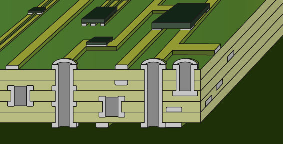
Blind vias are interconnects that start on an external layer and terminate on an internal layer, remaining invisible from the opposite side of the board. Unlike through-hole vias, which span the full board thickness, blind vias conserve space and reduce parasitic inductance for high-speed signals. They are particularly valuable in multilayer boards where routing density demands efficient vertical transitions. Buried vias, by contrast, connect only internal layers, complementing blind vias in complex stackups. The adoption of blind vias has grown with the rise of HDI PCBs used in smartphones, wearables, and automotive electronics. Their importance lies in enabling finer pitch components and shorter signal paths, which directly impact signal integrity and thermal management.
In PCB design, blind vias allow engineers to escape surface constraints and access inner routing layers without wasting real estate on unnecessary holes. This efficiency translates to smaller board sizes or more features within the same footprint. However, improper design can lead to fabrication challenges, such as drill breakout or inadequate plating. Manufacturers favor blind vias in sequential build-up processes, where layers are laminated in stages to expose specific depths. Overall, mastering blind via rules bridges the gap between innovative designs and production feasibility.
Key Technical Principles of Blind Via Design
The core of blind via rules revolves around aspect ratio, which is the ratio of via depth to drill diameter. A favorable aspect ratio ensures uniform copper plating and minimizes voids during electroless and electrolytic processes. IPC-2226 provides guidelines for high-density interconnects, emphasizing conservative ratios for microvias typically around 1:1 or less to promote reliability. Exceeding these limits risks incomplete filling and mechanical weakness, especially in stacked configurations. Engineers calculate aspect ratio based on the exact layer pair targeted, accounting for material thickness and drill tolerance.
Pad design forms another pillar of blind via rules. The annular ring, or landing pad, must exceed the finished hole size by a specified margin to accommodate drill wander and etching tolerances. Minimum pad diameters scale with via size, ensuring sufficient copper for current carrying and solder joint integrity. In PCB design software, rules enforce these clearances to prevent shorts or opens during fabrication. Anti-pad sizes on opposing layers also require attention to avoid residue trapping.
Via protection strategies influence long-term performance. Options include tenting with solder mask, plating over, or filling with conductive epoxy, each suited to specific environments. Tenting shields vias from contaminants, while filling supports vias-in-pad for BGA components. These choices align with IPC-6012 performance specifications, which dictate plating thickness and hole wall quality for different product classes.
Drill type selection dictates precision and cost. Mechanical drilling suits larger blind vias above 0.15 mm diameter, while laser ablation excels for microvias under 0.10 mm, vaporizing dielectric without mechanical stress. Hybrid approaches combine both for optimized stackups. Each method imposes unique rules on depth control and cleanup to prevent smear or debris.
Blind Via Manufacturing Considerations
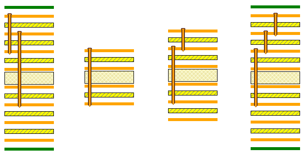
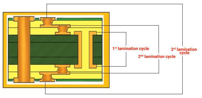
PCB manufacturing of blind vias demands sequential lamination, where cores are built incrementally and vias drilled post-lamination. This process isolates via depths, allowing precise control but increasing cycle time and cost compared to standard through vias. Registration accuracy between layers becomes paramount, as misalignment exceeds tolerances leading to stubby connections or breakthroughs. Manufacturers specify capabilities in terms of minimum via size, layer count, and build type, such as 1-n-1 or 2-n-2 configurations.
Plating uniformity poses a significant challenge due to the shallower depth of blind vias. Electrolytic copper deposition must achieve at least 20 microns on hole walls without barrel cracking, as outlined in industry performance standards. Post-plating inspection verifies continuity and resistance, often using automated optical or electrical testing. Aspect ratio constraints tighten further in production, typically limited to 1:1 for reliability under thermal cycling.
Material selection impacts blind via success. Low-loss dielectrics with controlled CTE match copper to reduce stress at interfaces. Prepreg thickness uniformity ensures consistent depths across panels. In high-volume manufacturing, panel-level processing amplifies the need for design rules that scale from prototype to production.
Yield optimization relies on design-for-manufacturability (DFM) checks. Excessive blind via density strains drill throughput and increases scrap from breakout. Staggered or filled vias mitigate risks in dense areas. Collaboration between design and fabrication teams early in the process refines rules to balance performance and cost.
Best Practices for Implementing Blind Via Rules in PCB Design
Start with stackup planning to minimize blind via spans, preferring single-layer transitions over multi-layer. Use simulation tools to verify signal integrity, as blind vias reduce stubs that cause impedance discontinuities. Enforce rules for minimum land sizes and clearances in design databases, scaling by fabrication class. For Class 3 assemblies, adopt conservative margins per IPC guidelines to withstand harsh environments.
Opt for filled or plugged vias in high-reliability applications to eliminate air pockets and enhance thermal conductivity. Conduct thermal modeling to predict hotspots around via clusters. During routing, prioritize blind vias for high-speed nets, fanning out BGA balls efficiently. Document via types and depths in fabrication drawings for unambiguous interpretation.
Test prototypes rigorously with cross-sectioning to validate plating and depth. Iterate designs based on feedback, adjusting rules for specific materials or processes. In team environments, standardize blind via libraries to ensure consistency across projects. These practices elevate PCB design from feasible to exceptional.
Common Challenges and Troubleshooting
One frequent issue is via cratering, where plating delaminates due to excessive aspect ratios or contaminated surfaces. Mitigate by selecting clean drilling methods and optimizing desmear processes. Another challenge involves breakout in sequential builds, addressed through precise depth control and fiducial alignment.
Signal integrity degradation from via stubs requires staggering or back-drilling alternatives. Thermal expansion mismatch leads to cracking under reflow; choose matched CTE materials. Troubleshooting starts with failure analysis, including dye-and-peel for adhesion and C-SAM for voids.
Conclusion
Blind via rules form the backbone of advanced PCB design, enabling compact, high-performance boards essential for today's electronics. By prioritizing aspect ratios, pad geometries, and manufacturing processes, engineers ensure reliability across the product lifecycle. Adhering to standards like IPC-2226 and IPC-6012 guarantees compliance and quality. Integrating these principles early prevents costly redesigns and accelerates time-to-market. Ultimately, thoughtful application of blind via rules optimizes both PCB design and manufacturing outcomes.
FAQs
Q1: What are the primary blind via rules in PCB design?
A1: Blind via rules emphasize aspect ratios not exceeding 1:1, adequate annular rings larger than finished hole sizes, and precise layer targeting. Designers must account for drill tolerances and plating uniformity to avoid voids. These rules, guided by IPC-2226, support HDI layouts by enabling dense routing without through-hole interference. Following them ensures signal integrity and mechanical strength.
Q2: How do blind via rules affect PCB manufacturing processes?
A2: Blind via rules necessitate sequential lamination, increasing steps but allowing controlled depths. Manufacturers limit via sizes and densities based on drill capabilities, with laser for microvias and mechanical for larger ones. Plating challenges demand uniform deposition, impacting yield. Adhering to these rules streamlines production and reduces defects in high-volume runs.
Q3: Why is aspect ratio critical in blind via rules for PCB design?
A3: Aspect ratio dictates plating quality, with ratios over 1:1 risking incomplete copper fill and reliability failures. IPC-2226 recommends conservative limits like 0.75:1 for microvias to ensure void-free walls. This principle directly influences stackup choices and via spans. Proper management enhances thermal and electrical performance in dense boards.
Q4: Can blind vias be used in all PCB types during manufacturing?
A4: Blind vias suit multilayer HDI boards but require advanced capabilities not universal in standard fabrication. Rules vary by class, with Class 3 demanding tighter tolerances. Sequential processes add cost, so evaluate against through-via alternatives. They excel in space-constrained designs, improving density when rules are followed precisely.
FAQs
IPC-2226A — Sectional Design Standard for High Density Interconnect Printed Boards. IPC, 2017
IPC-6012E — Qualification and Performance Specification for Rigid Printed Boards. IPC, 2020
IPC-2221C — Generic Standard on Printed Board Design. IPC, 2023


