Introduction
In modern PCB assembly, especially for high-density designs with ball grid array components, reliability hinges on robust solder joints. Solder wicking occurs when molten solder is drawn into open vias during reflow, depleting the solder volume needed for proper joint formation. This issue often leads to weak connections, increased voiding, and potential failures under thermal or mechanical stress. Contamination in vias exacerbates these problems by trapping flux residues or debris, which can compromise long-term performance. Via filling emerges as a critical solution for solder wicking prevention, ensuring vias do not interfere with soldering processes. By addressing these challenges head-on, engineers can achieve higher assembly yields and enhanced board reliability.
Understanding Solder Wicking and Via Contamination
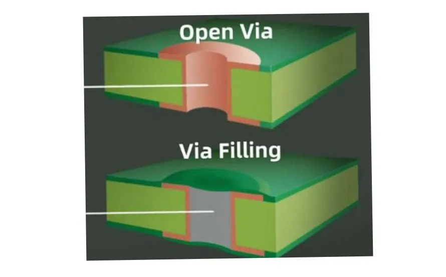
Solder wicking refers to the capillary action that pulls liquid solder into the barrel of an unfilled via, particularly under via-in-pad configurations common in BGA assembly. This phenomenon reduces the available solder for fillet formation around the component pad, resulting in incomplete joints prone to cracking. Engineers often observe this during reflow soldering, where surface tension and wetting properties drive the solder flow. Via contamination compounds the issue, as open holes collect solder paste particles, flux vapors, or environmental debris during fabrication and assembly. These contaminants can outgas during reflow, creating voids or bridges that undermine joint integrity.
The relevance of these problems intensifies in compact electronics, where space constraints demand vias directly under component pads. Weak solder joints from wicking lead to higher failure rates in thermal cycling tests, impacting overall product lifespan. Preventing contamination in vias maintains clean surfaces for consistent wetting and flow. For electric engineers troubleshooting assemblies, recognizing these failure modes early allows for proactive design adjustments. Ultimately, addressing solder wicking and contamination directly boosts PCB reliability in demanding applications.
Mechanisms Behind Solder Wicking and Contamination Risks
Capillary forces dominate solder wicking, where the narrow via geometry promotes rapid solder migration once wetting begins on the plated walls. During reflow, temperatures melt the solder paste, and the via's surface finish influences how aggressively solder is drawn in. Non-optimal plating or residues accelerate this, starving the pad-solder interface. Engineers must consider via aspect ratios and plating thickness, as steeper walls heighten wicking tendencies. Contamination arises from incomplete cleaning post-fabrication, leaving ionic residues that promote corrosion over time.
Thermal expansion mismatches between via fill materials and copper exacerbate risks if vias remain open. Flux activation during soldering releases volatiles that condense in vias, fostering electrochemical migration. IPC-7095 outlines design considerations for BGA vias to mitigate these effects, emphasizing controlled via treatments. In practice, unfilled vias under BGAs show higher void percentages in X-ray inspections, signaling joint weakness. Understanding these mechanisms guides engineers toward via filling for reliable soldering.
How Via Filling Addresses These Challenges
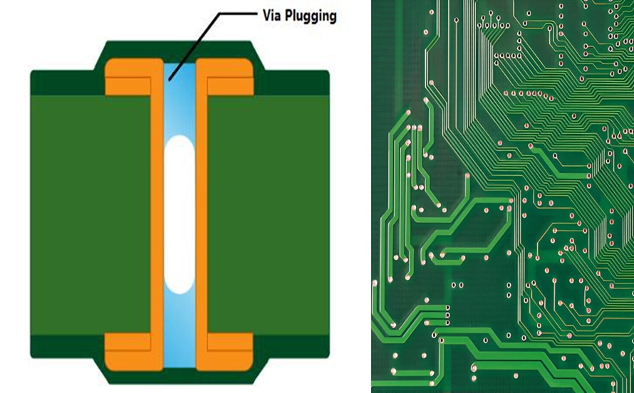
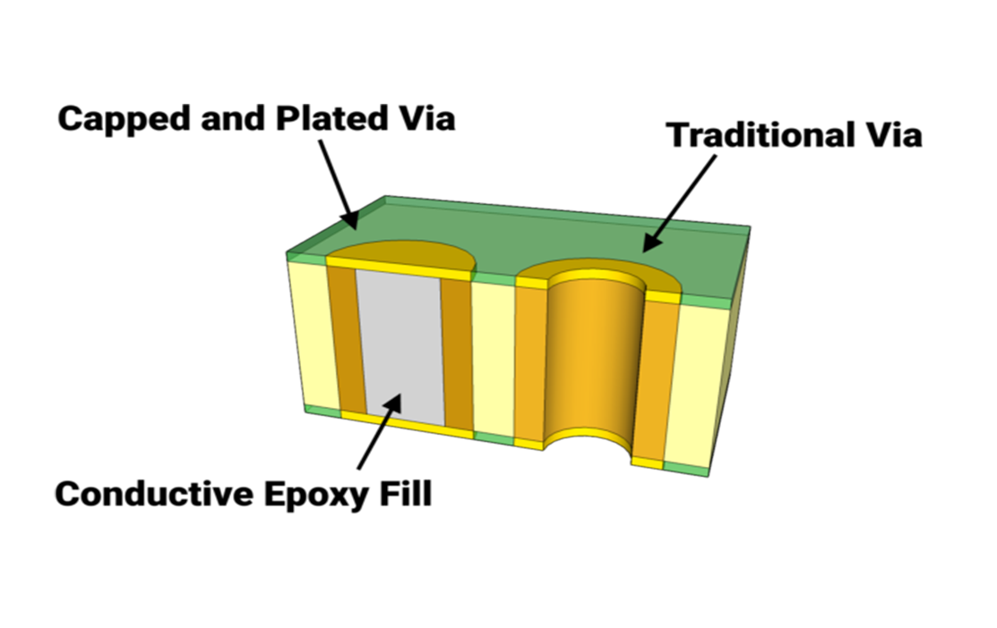
Via filling completely occludes the via barrel with conductive or non-conductive materials, blocking solder entry and eliminating wicking paths. Non-conductive fills, such as epoxy resins, provide mechanical support without altering electrical paths, ideal for signal integrity. Conductive copper filling maintains via conductivity while planarizing the surface for uniform stencil printing. This approach ensures full solder volume retention on pads, improving solder joint strength with via filling. Post-fill plating or capping seals the structure, preventing outgassing or ingress.
IPC-4761 classifies via filling types, including fully filled and covered configurations that meet reliability criteria for high-density boards. In BGA assembly via filling, this prevents solder loss, yielding flatter joints resistant to shear forces. Contamination risks drop as filled vias resist trapping residues during wave or reflow processes. Engineers report smoother assembly flows with reduced rework when implementing these methods. Overall, via filling transforms potential failure points into robust interconnects.
Best Practices for Implementing Via Filling
Select via filling based on design needs: non-conductive for cost-effective signal vias, conductive for power or ground planes. Specify fill materials compatible with subsequent processes like ENIG or OSP finishes to avoid adhesion issues. During fabrication, ensure complete fill without dimples exceeding allowable limits per board qualification specs. For BGA sites, integrate via filling early in the stackup to support dogbone or filled via-in-pad layouts. Test assemblies with shear and thermal cycle evaluations to verify joint performance.
In troubleshooting, inspect for fill voids using cross-section analysis before assembly. Adjust stencil apertures to compensate for any minor fill protrusion, maintaining paste volume consistency. Collaborate with fabricators on process controls for uniform filling, especially in high-aspect-ratio vias. These steps align with solder wicking prevention strategies, minimizing defects. Regular process audits confirm via integrity across production runs.
Troubleshooting Common Issues in Via-Filled Assemblies
Engineers often encounter incomplete fills leading to residual wicking, diagnosable via dye-and-peel tests or automated optical inspection. If joints show head-in-pillow defects, check for fill outgassing by ramping reflow profiles slower. Contamination post-filling manifests as delamination; mitigate with plasma cleaning pre-plating. In BGA rework, filled vias withstand higher temperatures without cracking, unlike open ones. Document failure modes in assembly logs to refine future designs.
Case insights from high-volume production reveal that via filling reduces BGA yield losses by stabilizing joints under vibration. One common pitfall is over-specifying fill thickness, causing pad non-planarity; balance with fab capabilities. Cross-reference with IPC-6012 for acceptance on rigid boards ensures compliance. Proactive via filling resolves these pain points effectively.
Conclusion
Via filling stands as a proven method for solder wicking prevention and preventing contamination in vias, directly enhancing PCB reliability. By blocking capillary paths and sealing against residues, it ensures robust BGA solder joints capable of enduring operational stresses. Engineers benefit from stronger interconnections, fewer assembly defects, and extended field life. Integrating best practices around standards like IPC-4761 and IPC-7095 delivers consistent results. Prioritizing via filling in high-density designs pays dividends in performance and manufacturability.
FAQs
Q1: What is the primary benefit of via filling for reliable soldering in BGA assembly?
A1: Via filling for reliable soldering prevents molten solder from wicking into vias under BGA pads, preserving full solder volume for strong fillet formation. This reduces voiding and head-in-pillow defects common in reflow processes. Engineers achieve higher joint integrity without altering component placement, streamlining high-volume production. Practical implementation involves specifying non-conductive fills early in design.
Q2: How does via filling contribute to solder wicking prevention?
A2: Solder wicking prevention through via filling eliminates open barrels that draw in liquid solder via capillary action. Filled vias maintain pad planarity, ensuring even paste deposition and reflow. This approach avoids weak joints prone to fatigue cracking under thermal cycling. Troubleshooting focuses on verifying complete occlusion post-fabrication for optimal results.
Q3: Why is preventing contamination in vias critical for PCB reliability?
A3: Preventing contamination in vias stops flux residues and particles from trapping, which cause outgassing and corrosion during assembly. Filled vias seal these areas, promoting clean reflow and long-term stability. Electric engineers note fewer electrochemical failures in humid environments. Combine with proper cleaning for comprehensive protection.
Q4: Can via filling improve solder joint strength with via filling techniques?
A4: Improving solder joint strength with via filling ensures no solder loss, yielding thicker fillets resistant to shear and drop tests. Non-conductive or copper fills support this without signal distortion. Best practices include process validation for uniform joints across boards. This enhances overall assembly yield in demanding applications.
References
IPC-4761 - Via Protection and Covering for Printed Circuit Boards. IPC
IPC-7095D - Design and Assembly Process Implementation for Ball Grid Arrays (BGAs). IPC
IPC-6012E - Qualification and Performance Specification for Rigid Printed Boards. IPC, 2017
J-STD-001H - Requirements for Soldered Electrical and Electronic Assemblies. IPC/JEDEC, 2020


