Introduction
Printed Circuit Board (PCB) manufacturing is a cornerstone of modern electronics, enabling the functionality of devices across industries. For electrical engineers, the process presents a range of challenges that can impact design performance and production efficiency. Key issues often revolve around physical access to components, electrical signals and routing path optimization, and ensuring reliable signal communication and power supply. These elements are critical to achieving a functional and durable PCB. This article explores these hurdles in detail, offering insights into their causes and practical solutions. By addressing these challenges, engineers can improve design outcomes and streamline manufacturing processes while adhering to industry standards. The discussion aims to equip professionals with the knowledge needed to navigate complex PCB production landscapes effectively.
Why PCB Manufacturing Challenges Matter
PCB manufacturing is not merely about assembling components on a board. It is a complex process that directly affects the performance, reliability, and cost of electronic products. Challenges in areas like physical access to components can lead to assembly errors or maintenance difficulties. Issues with electrical signals and routing path design can cause signal degradation or interference, compromising device functionality. Similarly, problems in signal communication and power supply can result in system failures or inefficiencies. For electrical engineers, understanding these obstacles is vital to meeting project specifications and ensuring product quality. Overcoming these issues also reduces production delays and minimizes costly rework, ultimately supporting innovation in electronics development.
Technical Challenges in PCB Manufacturing
Physical Access to Components
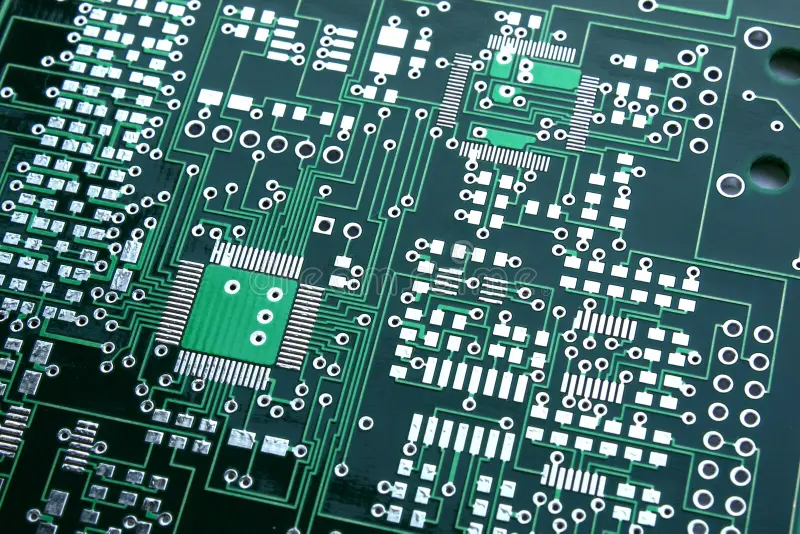
One significant challenge in PCB manufacturing is ensuring physical access to components during assembly, testing, and maintenance. As designs become more compact to meet miniaturization demands, components are placed closer together, often in high-density layouts. This can restrict access for soldering tools, probes, or even visual inspection. In multilayer boards, inner layers may house critical components that are impossible to reach without specialized equipment.
The issue of physical access also extends to repair and rework scenarios. If a component fails, accessing it without damaging adjacent parts or the board itself can be difficult. This challenge is compounded in designs with surface-mount technology, where components are smaller and more delicate. Engineers must balance the need for compact designs with the practical requirement for accessibility during manufacturing and beyond.
Electrical Signals and Routing Path Complexities
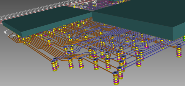
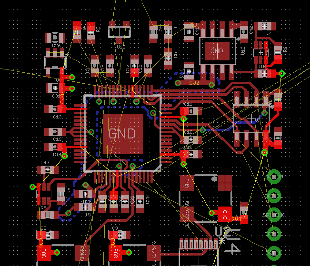
Another critical area of concern is managing electrical signals and routing path configurations. The routing path determines how signals travel between components, and poor design can lead to issues like crosstalk, impedance mismatches, or signal delays. As operating frequencies increase in modern electronics, maintaining signal integrity becomes more challenging. High-speed signals are particularly susceptible to interference if traces are not properly spaced or shielded.
Routing in multilayer PCBs adds further complexity. Engineers must navigate limited space while avoiding vias that can introduce parasitic capacitance or inductance. Additionally, ensuring that critical nets have the shortest possible paths is essential to minimize latency. Failure to optimize electrical signals and routing path design can result in performance degradation, especially in applications requiring precise timing or high data rates.
Related Reading: High Frequency PCB Routing Techniques: Minimizing Signal Loss and Interference
Signal Communication and Power Supply Issues
Reliable signal communication and power supply are foundational to PCB functionality, yet they present persistent challenges. Signal communication issues often arise from electromagnetic interference or improper grounding techniques. If ground planes are not adequately designed, noise can disrupt signal transmission, leading to data errors or system instability. This is particularly problematic in mixed-signal designs, where analog and digital signals coexist.
Power supply challenges include ensuring stable voltage delivery across the board. Voltage drops or insufficient current capacity can cause components to malfunction. Additionally, power distribution networks must be designed to handle peak loads without overheating or causing electromagnetic emissions. Engineers must also consider decoupling capacitors and their placement to filter noise effectively. Addressing signal communication and power supply concerns requires meticulous planning and adherence to best practices.
Practical Solutions and Best Practices
Enhancing Physical Access to Components
To mitigate issues with physical access to components, engineers can adopt several strategies during the design phase. First, prioritize component placement by grouping related parts together and leaving sufficient clearance for tools and probes. For high-density designs, consider using modular layouts that allow easier access to specific sections. Additionally, incorporating test points in accessible locations can simplify diagnostics without requiring direct component access.
During manufacturing, using automated assembly equipment designed for precision can reduce errors in tight spaces. For multilayer boards, ensure that design files clearly indicate critical access areas to guide assembly processes. Following standards such as IPC-2221B, which provides guidelines for PCB design, can help in establishing practical layouts that balance density with accessibility.
Optimizing Electrical Signals and Routing Path
To address challenges with electrical signals and routing path, engineers should focus on signal integrity from the outset. Use controlled impedance routing for high-speed signals to prevent mismatches, and maintain consistent trace widths and spacing. Implementing differential pair routing for critical signals can minimize crosstalk and improve noise immunity. Additionally, avoid sharp bends in traces to reduce signal reflection risks.
Simulation tools can aid in predicting and resolving routing issues before fabrication. Layer stackup planning is also crucial; dedicate specific layers to ground planes to shield sensitive signals. Adhering to guidelines in IPC-2251, which covers high-speed design principles, ensures that routing paths support optimal electrical performance. These practices help maintain signal quality across diverse applications.
Improving Signal Communication and Power Supply
For reliable signal communication and power supply, start with a robust grounding strategy. Use continuous ground planes to provide a low-impedance return path for signals, reducing noise. Separate analog and digital grounds where necessary to prevent interference. For power distribution, design wide traces or power planes to handle current demands and minimize voltage drops.
Place decoupling capacitors close to power pins of active components to stabilize voltage levels. Ensure proper via placement to connect power layers without introducing unnecessary resistance. Following standards like IPC-2152, which addresses current-carrying capacity and thermal management, can guide power supply design. These steps collectively enhance signal communication and power delivery reliability.
Related Reading: Optimizing Power and Ground Planes in Stackup for Better Circuit Performance
Insights for Electrical Engineers
For electrical engineers, overcoming PCB manufacturing challenges requires a blend of theoretical knowledge and practical experience. Start by integrating design for manufacturability principles early in the process. This means collaborating with manufacturing teams to understand their constraints and capabilities. Regularly review designs against industry standards to ensure compliance and performance.
Testing and validation are also critical. Conduct thorough signal integrity analysis and power distribution simulations to identify potential issues before production. Iterative prototyping can help refine designs, especially for complex boards with high-speed requirements. By focusing on physical access to components, electrical signals and routing path optimization, and robust signal communication and power supply, engineers can achieve reliable and efficient PCB outcomes.
Conclusion
PCB manufacturing presents multifaceted challenges that electrical engineers must navigate to ensure product success. Issues related to physical access to components can hinder assembly and maintenance, while complexities in electrical signals and routing path design impact performance. Additionally, maintaining effective signal communication and power supply is essential for system stability. By implementing strategic solutions and adhering to established standards, engineers can address these obstacles effectively. A proactive approach, grounded in best practices, ensures that PCBs meet the demands of modern electronics while supporting innovation and reliability in the field.
FAQs
Q1: How does physical access to components affect PCB manufacturing?
A1: Physical access to components is crucial in PCB manufacturing as it impacts assembly, testing, and repair processes. Limited access in high-density designs can lead to soldering errors or difficulties in diagnostics. Engineers can mitigate this by planning layouts with adequate spacing and accessible test points, ensuring smoother production and maintenance without compromising design compactness.
Q2: What are common issues with electrical signals and routing path in PCBs?
A2: Electrical signals and routing path challenges often include crosstalk, impedance mismatches, and signal delays, especially in high-speed designs. Poor routing can degrade performance by introducing interference or latency. Solutions involve controlled impedance traces, differential pairing, and simulation tools to optimize paths, ensuring signal integrity across the board for reliable operation.
Q3: How can signal communication and power supply be improved in PCB design?
A3: Improving signal communication and power supply involves using solid ground planes to reduce noise and separate analog and digital signals. For power, wide traces and strategically placed decoupling capacitors ensure stable delivery. Following industry guidelines helps manage current loads and minimize interference, enhancing overall PCB reliability for various applications.
Q4: Why is addressing power supply challenges critical in PCB manufacturing?
A4: Power supply challenges, like voltage drops or insufficient current, can cause component failures or system instability in PCBs. A well-designed power distribution network with adequate trace sizing and capacitor placement prevents these issues. Ensuring stable power supply is vital for maintaining performance, especially in complex designs with high power demands.
References
IPC-2221B — Generic Standard on Printed Board Design. IPC, 2012.
IPC-2251 — Design Guide for High-Speed Controlled Impedance Circuit Boards. IPC, 2003.
IPC-2152 — Standard for Determining Current Carrying Capacity in Printed Board Design. IPC, 2009.


