Introduction
Printed circuit boards form the backbone of modern electronics, and their reliability hinges on precise manufacturing choices. PCB edge plating, also known as edge metallization, plays a critical role in enhancing board integrity, especially in demanding applications like high-frequency circuits and edge-card connectors. Electrical engineers must select appropriate PCB edge plating materials to ensure electrical continuity, mechanical strength, and protection against environmental factors. Common options include copper plating as the base layer, overlaid with finishes such as gold plating or ENIG finish. This article explores these surface finishes for PCB, their properties, and selection criteria aligned with industry practices. Understanding these elements helps engineers optimize performance while adhering to manufacturing constraints.
What Is PCB Edge Plating and Why Does It Matter?
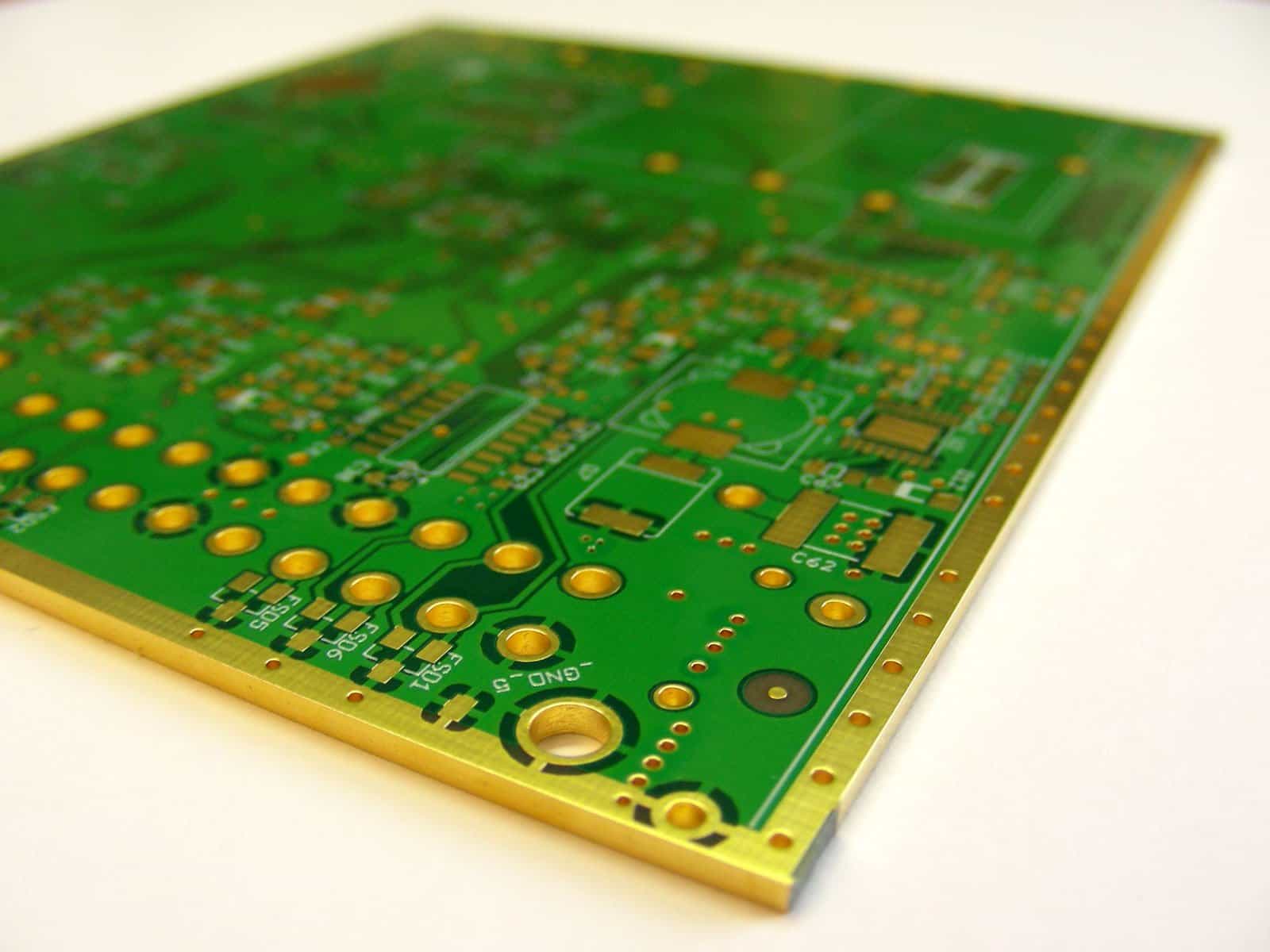
PCB edge plating involves depositing a conductive metal layer, typically copper, along the outer edges of a printed circuit board. This process extends from the top surface through the board thickness to the bottom, creating a robust metallized edge. Engineers apply edge plating to achieve multiple objectives, including improved solderability for edge connectors, electromagnetic interference shielding, and enhanced structural rigidity. In applications like backplanes or modular systems, unplated edges risk cracking under thermal stress or vibration, leading to failures. Proper material selection prevents oxidation and ensures reliable current paths across the board perimeter. Factory processes mask non-edge areas before electrolytic plating, ensuring uniform coverage.
The relevance of PCB edge plating materials intensifies in high-reliability sectors such as aerospace and telecommunications. Without adequate plating, boards may exhibit warpage or delamination during assembly. Standards like IPC-6012 outline qualification requirements for plating adhesion and thickness, guiding manufacturers toward consistent quality. Engineers benefit from edge plating by reducing signal integrity issues in dense layouts. Ultimately, choosing the right materials balances cost, durability, and performance for long-term board functionality.
Key Materials for Base Plating: Focus on Copper
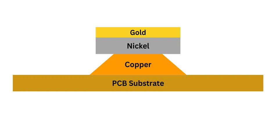
Copper remains the primary material for PCB edge plating due to its excellent conductivity and cost-effectiveness. In the plating process, a copper bus or tab connects the edge to the board's power or ground planes, allowing electrolytic deposition. This base layer typically achieves thicknesses of 25 to 50 microns, providing sufficient mechanical support without excessive weight. Copper plating excels in high-current applications where low resistance is paramount. However, bare copper oxidizes quickly, necessitating protective surface finishes for PCB. Manufacturers control plating parameters like current density to minimize voids and ensure uniformity.
Copper's ductility accommodates board flexing during handling or operation, reducing crack propagation risks. Electrical engineers specify copper edge plating for its compatibility with standard fabrication flows, integrating seamlessly with through-hole plating. Variations in copper grain structure influence long-term reliability under thermal cycling. Factory inspections verify plating continuity using continuity testers post-deposition. Selecting high-purity copper foils upstream prevents impurities that could compromise edge quality.
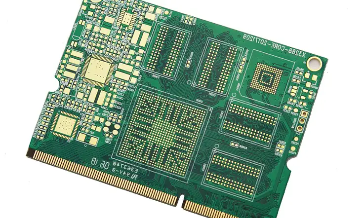
Surface Finishes for PCB Edge Plating: Options and Properties
Surface finishes for PCB protect the underlying copper while enabling soldering or mating connections. ENIG finish, or electroless nickel immersion gold, deposits a nickel barrier layer topped with thin gold, offering superior corrosion resistance. This finish suits edge plating in humid environments, as gold prevents oxidation diffusion to the copper. Nickel thickness typically ranges from 3 to 6 microns, with gold at 0.05 to 0.1 microns for optimal solderability. ENIG maintains flatness critical for high-density edge connectors, avoiding the unevenness of lead-free HASL.
Gold plating provides an alternative for high-wear applications like finger contacts. Hard gold, electroplated over nickel underlayers, delivers abrasion resistance for repeated insertions. Soft gold variants prioritize solder joint reliability in less demanding scenarios. Engineers compare gold plating to ENIG based on contact force requirements and lifecycle expectations. Immersion silver or tin finishes offer economical options for non-critical edges, though they demand controlled storage to avoid tarnishing. Each finish influences assembly yields, with factory data showing ENIG's edge in black pad mitigation.
- ENIG Finish — Benefits: Corrosion resistance, flat surface, solderable; Applications: High-reliability edge connectors, RF modules; Limitations: Higher cost, potential phosphor issues.
- Gold Plating — Benefits: Wear resistance, conductivity; Applications: Gold fingers, high-cycle mating; Limitations: Expensive, thickness control challenges.
- Immersion Silver — Benefits: Low cost, excellent solderability; Applications: General shielding edges; Limitations: Tarnish-prone, short shelf life.
- HASL (Lead-Free) — Benefits: Robust, inexpensive; Applications: Mechanical edges, non-contact; Limitations: Uneven surface, not for fine-pitch.
This list summarizes common surface finishes for PCB, aiding material selection.
Factors Influencing Material Selection for PCB Edge Plating
Engineers evaluate several factors when choosing PCB edge plating materials, starting with operational environment. Harsh conditions like high humidity or salt exposure favor ENIG finish or gold plating for barrier protection. Thermal management plays a key role, as mismatched coefficients of thermal expansion between plating and laminate cause stress. Copper plating's compatibility with FR-4 laminates minimizes this risk. Cost considerations balance initial expense against lifecycle savings, with ENIG justifying premiums in mission-critical designs.
Electrical performance dictates choices, particularly impedance control near edges. Standards such as IPC-A-600 define acceptability criteria for plating coverage and voids, ensuring compliance. Board thickness and stack-up influence plating uniformity, requiring adjusted process parameters. Engineers simulate stress via finite element analysis to predict edge reliability. Manufacturing yield data from factories highlights copper plating's robustness across volumes. Procurement teams weigh lead times, as gold plating may extend schedules due to specialized baths.
Best Practices in PCB Edge Plating Manufacturing
Adhere to sequential process control for optimal results. Begin with precise edge masking using photoresist or dry film to expose only target areas. Electrolytic copper plating follows panel or pattern sequencing, with post-plating etch removing excess. Apply surface finishes promptly to avoid copper exposure. Factories monitor bath chemistry, maintaining copper sulfate concentrations for even deposition. Peel strength tests verify adhesion per industry guidelines.
Design for manufacturability includes specifying bevels on edges to reduce plating shadows. Avoid sharp corners that trap plating solutions, promoting uniform coverage. Electrical engineers collaborate with fabricators early, sharing gerber files with edge plating annotations. Post-plating inspections employ X-ray or cross-sectioning for thickness validation. IPC-2221 provides design guidelines for edge features, preventing common pitfalls like insufficient bus width. These practices yield high first-pass yields and reliable boards.
Common Challenges and Troubleshooting in Edge Plating
Uneven plating thickness arises from poor current distribution, resolvable by panel rotation or thief areas. Voids or dog-boning occur in thick boards, mitigated by pulse plating techniques. Black pad defects in ENIG finish stem from excessive nickel phosphorus, controlled via optimized immersion times. Engineers troubleshoot via failure analysis, sectioning samples for microscopy. Corrosion post-assembly signals inadequate gold coverage, prompting finish specification reviews.
Factory-driven solutions include in-line monitoring with eddy current gauges for real-time thickness feedback. Thermal shock testing simulates assembly stresses, identifying weak edges early. Documentation of process windows ensures repeatability across lots. Addressing these challenges upholds quality in PCB edge plating materials selection.
Conclusion
Selecting the right PCB edge plating materials demands a nuanced understanding of copper plating, gold plating, ENIG finish, and other surface finishes for PCB. Copper provides the conductive foundation, while finishes ensure longevity and performance. Factors like environment, standards compliance, and manufacturing feasibility guide choices. By following best practices and referencing IPC guidelines, engineers achieve robust, reliable boards. This approach minimizes failures, optimizes costs, and supports advanced electronics designs.
FAQs
Q1: What are the most common PCB edge plating materials?
A1: Copper plating serves as the base for most PCB edge plating due to its conductivity and ductility. Protective layers like ENIG finish or gold plating follow to prevent oxidation. Selection depends on application needs, such as shielding or connectors. Factories ensure thickness uniformity per standards for reliability.
Q2: Why choose ENIG finish for surface finishes for PCB edges?
A2: ENIG finish offers excellent corrosion resistance and solderability for PCB edges in humid or high-reliability settings. The nickel barrier blocks copper diffusion, while thin gold enables clean joints. It maintains planarity for precise mating. Drawbacks include cost, but benefits outweigh in demanding uses.
Q3: How does gold plating compare to copper plating in edge applications?
A3: Gold plating provides superior wear resistance over copper for frequent contacts like edge fingers. Copper handles bulk conduction economically, often underplated before gold. Combine them for balanced performance. Engineers specify based on cycles and environment.
Q4: What standards guide PCB edge plating materials selection?
A4: IPC-6012 and IPC-A-600 define plating quality, thickness, and acceptability for edges. IPC-2221 offers design rules. Compliance ensures manufacturability and performance.
References
IPC-6012E — Qualification and Performance Specification for Rigid Printed Boards. IPC, 2015
IPC-A-600K — Acceptability of Printed Boards. IPC, 2020
IPC-2221B — Generic Standard on Printed Board Design. IPC, 2012


