Introduction
Component placement forms the foundation of any successful PCB layout, directly influencing signal integrity, manufacturability, and overall performance. In Altium Designer, mastering this process allows engineers to achieve optimized designs that minimize routing challenges and ensure compliance with industry standards. This Altium component placement tutorial explores structured techniques to position components effectively, from initial synchronization to advanced interactive tools. Electric engineers will find value in the logical progression of steps that prioritize functionality and reliability. By following Altium best practices for component placement, designers can reduce iterations and enhance signal integrity from the outset. Proper placement sets the stage for efficient routing and robust boards.
Why Component Placement Matters in PCB Design
Component placement determines how well signals propagate without degradation, affecting crosstalk, impedance mismatches, and electromagnetic interference. Poor decisions early on lead to longer traces, more vias, and thermal hotspots, complicating high-speed designs. In complex boards, strategic grouping by function streamlines assembly and testing while adhering to guidelines like those in IPC-2221 for spacing and clearance. This step consumes up to 90 percent of design effort, as adjustments during routing become costly. Effective placement supports signal integrity by keeping critical nets short and return paths robust. Ultimately, it bridges schematic intent with physical realization, ensuring boards meet performance specs.
Manufacturers favor orderly layouts that facilitate automated pick-and-place machines and soldering processes. Clustering related components reduces handling errors and improves yield. For electric engineers, understanding these implications means fewer prototypes and faster time-to-market. Placement also impacts mechanical stability, with heavy components positioned to avoid board flexing.
Key Technical Principles of Component Placement
The core principle revolves around minimizing interconnect lengths while respecting electrical, thermal, and mechanical constraints. Components should group by signal type, such as analog sections isolated from digital to prevent noise coupling. Decoupling capacitors place near power pins of ICs to supply instantaneous currents and stabilize voltage rails. Reference points, defined in footprints, serve as anchors for precise positioning on grids.
Bounding boxes, derived from courtyard layers per IPC-7351, define collision zones during placement, preventing overlaps. Rotation optimization aligns pins for straight routing paths, reducing vias. Layer assignment considers double-sided efficiency, flipping orientations as needed. These mechanisms ensure designs scale from simple to high-density boards.
Signal paths benefit from facing pads, where connected components orient toward each other. Thermal dissipation spreads heat sources evenly, avoiding localized hotspots. Grid snapping enforces repeatability, aligning with fabrication tolerances.
Altium Component Placement Tutorial: Step-by-Step Guide
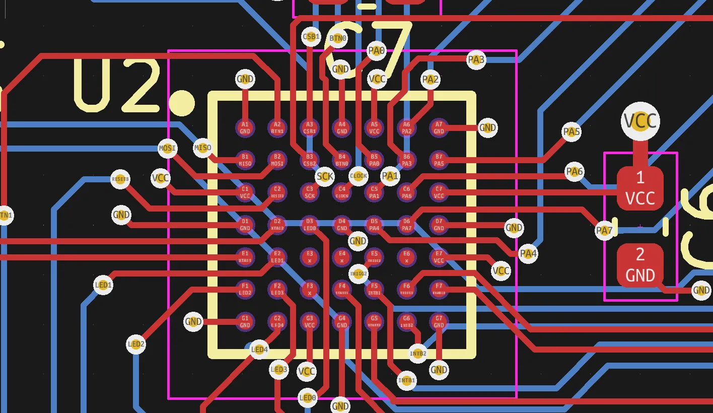
Begin by updating the PCB from the schematic using Design > Import Changes from schematic_name.SchDoc. This synchronizes footprints, nets, and parameters, placing primitives initially at default locations. Review the Engineering Change Order dialog, confirm actions, and execute to populate the board. Cross-probe between editors by selecting a component in the schematic; it highlights on the PCB for verification.
Access the PCB Editor and select Place > Component or use the Components panel to drag instances directly. During placement, press Tab to pause and edit properties like layer or rotation in the Properties panel. Cycle modes with R: Ignore Obstacles for freehand, Avoid Obstacles to skirt violations, or Push Obstacles to shove neighbors while maintaining clearances. Release the mouse to drop, observing the DRC real-time feedback.
For repositioning, use Edit > Move > Component, filtering by designator in the Choose Component dialog. Drag groups with Shift-select, aligning via green snap lines for centers or edges. Hold Ctrl for boundary snaps or Shift for pads. Optimize rotations via Tools > Optimize Component Rotation, normalizing to 0 degrees.
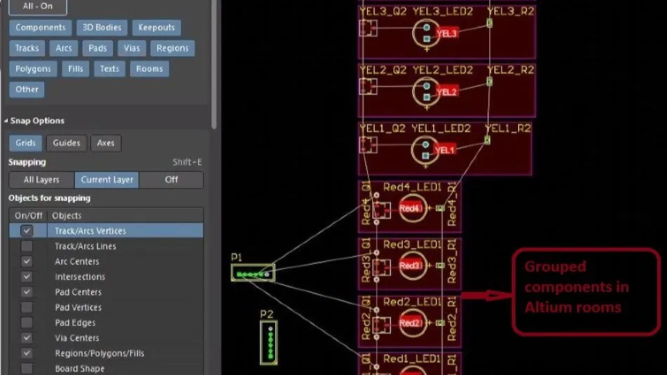
Rooms aid hierarchical designs: define via Place > Directives > Room, then Place > Component with room targeting. Arrange via Tools > Component Placement > Arrange Within Room for automatic fitting.
Altium Best Practices for Component Placement
Start with fixed elements like connectors and large ICs, locking them via the Properties panel to anchor the layout. Place high-power components centrally or dispersed for thermal balance, followed by passives nearby. Orient polarized parts uniformly and align similar packages for visual clarity and machine efficiency. Separate analog and digital zones over dedicated ground planes to uphold signal integrity.
Adhere to board edge clearances, typically 5-10 mm, and component spacing per design rules. Use both sides judiciously, placing SMDs primarily topside to cut assembly passes. Employ the PCB panel to sort by class, locking after positioning critical nets. Run DRC early, addressing violations like courtyard overlaps.
For dense boards, leverage Paste Array for repeated patterns and Swap Components for footprint exchanges. Align selections via right-click > Align, choosing space-equally or maintain-clearance options. These Altium best practices for component placement streamline workflows and boost reliability.
Ensuring Altium Signal Integrity Through Placement
Signal integrity hinges on short, matched-length traces and strong ground coupling, achievable via thoughtful placement. Position high-speed drivers and receivers close, minimizing stubs and reflections. Place bypass caps within 1-2 mm of IC power pins, routing short vias to planes. Group differential pairs with symmetric orientations for balanced routing.
In Altium, view net lengths and delays in Properties for interactive tuning. Assign components over reference planes, avoiding splits under signals. Use 3D body collision checks for precise clearances, enhancing impedance control. These strategies integrate Altium signal integrity directly into placement.
Monitor via counts; orient to reduce transitions. For RF sections, isolate with ground walls or moats.
Troubleshooting Common Placement Challenges
Overlaps trigger DRC errors; resolve by pushing in Avoid mode or manually nudging with arrow keys. Locked primitives halt moves; toggle in Properties. Misaligned grids cause snaps; adjust via View > Grids > Set Global. For hierarchical sheets, verify room memberships match sheets.
Thermal issues from clustered power arise; redistribute using average placement vectors shown during drags. Footprint mismatches update via Libraries panel right-click. Iterative checks with 3D view confirm physical feasibility.
Conclusion
Mastering component placement in Altium Designer transforms PCB layouts from adequate to exceptional, embedding efficiency and performance from the start. This tutorial equips electric engineers with tools like interactive modes, alignment aids, and DRC integration for flawless execution. Adhering to principles of grouping, optimization, and signal focus yields routable, manufacturable boards. Incorporate these steps routinely to elevate design quality. Future iterations benefit from locked baselines and parametric tweaks.
FAQs
Q1: What are the key steps in an Altium component placement tutorial?
A1: Transfer from schematic via Design > Import Changes, then place or move using Edit > Move > Component. Cycle modes with R for Push/Avoid Obstacles, aligning with snaps. Optimize rotations and run DRC to validate clearances. Lock fixed parts early for stability. This structured approach ensures logical layouts per engineering needs.
Q2: How do Altium best practices for component placement improve designs?
A2: Prioritize connectors first, group by function, and separate analog/digital zones. Align orientations and use both sides efficiently while respecting edges. Leverage rooms and auto-arrange for density. These practices shorten traces, enhance thermal flow, and align with IPC-2221 spacing, reducing errors.
Q3: Why focus on Altium signal integrity during component placement?
A3: Placement dictates trace lengths and plane coupling, critical for high-speed signals. Position caps near pins and pairs closely to minimize delays and crosstalk. Altium's net info and 3D checks aid real-time optimization. Early attention prevents costly reroutes.
Q4: What role do standards play in Altium component placement?
A4: Guidelines like IPC-7351 define courtyards for bounding boxes, ensuring no overlaps. IPC-2221 covers spacings for voltage and assembly. Integrate via design rules for compliance, boosting reliability without fabrication issues.
References
IPC-2221B — Generic Standard on Printed Board Design. IPC, 2012
IPC-7351C — Generic Requirements for Surface Mount Design and Land Pattern Standard. IPC, 2010
J-STD-001G — Requirements for Soldered Electrical and Electronic Assemblies. IPC, 2011