Why Create Your Own PCB Diagnostic Setup?
Printed Circuit Boards (PCBs) are the fundamental building blocks of almost all electronic devices, and thorough testing is critical to confirm their correct functionality before they are put into use. Commercial testing apparatus can be prohibitively expensive, often costing thousands of dollars, making them impractical for hobbyists or small-scale development projects. A DIY PCB testing setup offers a budget-friendly alternative, empowering you to effectively diagnose issues such as short circuits, broken traces, or malfunctioning components using readily available or easily acquired tools. Furthermore, constructing your own station provides complete control over its customization, allowing it to precisely meet your unique project requirements.
Essential Tools for a DIY PCB Tester
Before commencing construction of your PCB test jig, it’s crucial to assemble the necessary components and tools. Most of these items are readily accessible and affordable, making this a cost-effective diagnostic project.
Core Diagnostic Instruments
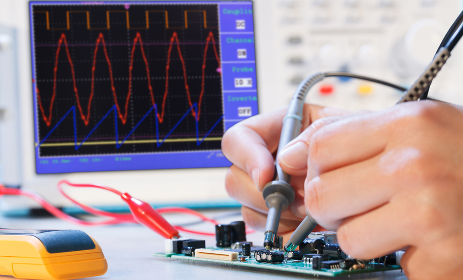
● Digital Multimeter: An indispensable tool for measuring voltage, current, and resistance. Opt for a model featuring a continuity test function to identify breaks in circuit traces; decent models typically range from $10 to $30.
● Adjustable Power Supply: A variable DC power supply (5V–12V, 1–2A) is needed to energize your quick turn PCB during testing. Affordable adjustable supplies can be found online for as little as $20.
● Precision Test Probes: Utilize fine-tipped probes or alligator clips to establish connections with small PCB pads and components. A set usually costs under $5.
● Pogo Pins: These spring-loaded pins create reliable, temporary contacts with designated test points on your PCB. A pack of 10 typically costs between $3 and $5.
Structural and Optional Components
● Jig Base: A stable platform such as a breadboard, acrylic sheet, or wood provides a foundation to mount your PCB and connect test points. A small breadboard is often priced around $5.
● Microcontroller (Optional): For those aspiring to an automated Arduino PCB tester, a microcontroller like an Arduino Uno (approximately 20-25) can streamline testing sequences.
● Assembly Tools: Essential miscellaneous items include a soldering iron, solder, various wires, and a magnifying glass for detailed inspection of minute components.
With a total budget often under $100, a fully functional homemade PCB tester capable of handling fundamental diagnostic tasks can be assembled.
Step-by-Step Guide to Constructing a PCB Test Jig
Once your tools are assembled, the next phase involves building the PCB test jig itself—a custom fixture designed to securely hold your PCB and simplify connections to test points.
Planning the Jig Layout
Begin by thoroughly analyzing the PCB you intend to test. Identify all crucial test points, including power rails, ground pads, and critical signal lines. Sketch a preliminary layout for your jig, ensuring that the pogo pins or probes will precisely align with these points. For repetitive testing of identical boards, meticulous precision at this stage is paramount for consistent results.
Selecting and Preparing the Base
Choose a robust material for the jig’s base, such as acrylic, wood, or even a modified breadboard. Precisely drill holes or mount holders for the pogo pins at the exact coordinates corresponding to your PCB’s test points. For a more refined setup, consider 3D printing a custom base if a printer is accessible.
Installing Pogo Pins and Clamping Mechanism
Securely insert the pogo pins into the prepared holes in the base. These spring-loaded pins will establish contact with the PCB without requiring soldering. Wire the opposite end of each pogo pin to a terminal or directly to your multimeter probes. Ensure precise pin alignment to prevent any damage to the PCB. To maintain stability during testing, integrate a simple clamping mechanism, such as rubber bands or small screws, to hold the board firmly against the pogo pins. Consistent contact is vital for accurate diagnostics.
Initial Jig Validation
Position your PCB onto the jig, apply power, and use your multimeter to verify voltages at key points. For example, if your board operates at 5V, confirm that the power rail registers close to 5V (ideally within a ±0.1V tolerance). Additionally, check for continuity on critical traces to confirm an unbroken circuit path.
Optimizing Your PCB Testing Workspace
Beyond constructing a jig, establishing an efficient PCB test environment is crucial for minimizing errors and maximizing diagnostic accuracy.
Workspace Organization and Safety
Maintain a meticulously organized workspace, arranging all tools and components on an anti-static mat to safeguard your multilayer PCBs from electrostatic discharge (ESD) damage. ESD mats are typically available for around $10. Ensure ample, bright illumination using a dedicated desk lamp or a magnifying lamp (costing about 15-30) to facilitate close inspection of small components and solder joints. For safety, always disconnect power before making any adjustments or connections to prevent shocks or short circuits.H3: Detailed Documentation
Keep a comprehensive record, either in a physical notebook or a digital log, of all test results. This should include readings like resistance values (e.g., noting a 1.2 kΩ reading versus an expected 1 kΩ) or voltage drops, which serve as invaluable future reference points. A well-structured test environment ensures both accurate diagnostics and the protection of your equipment and yourself.
Automating Diagnostics with an Arduino PCB Tester
For those aiming to elevate their DIY PCB testing capabilities, integrating an Arduino can automate repetitive tasks and provide digital readouts of test results. A microcontroller like Arduino can measure voltages, conduct continuity checks, and even log data to a computer.
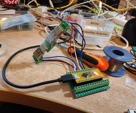
Assembling Arduino Components and Coding Basics
Begin by gathering necessary Arduino components, including an Arduino board (e.g., Uno or Nano, priced at 20-25), a compact LCD display (5-10) for output, resistors for voltage divider circuits, and jumper wires. Optionally, a buzzer can be added for audible continuity alerts. Program the Arduino to acquire analog voltage readings from specific pins connected to your PCB’s test points. For instance, employ the analogRead() function to measure a signal line expected to carry 3.3V. If the reading falls outside a defined tolerance (e.g., ±0.2V), the Arduino can activate a warning on the LCD or through the buzzer.H3: Integrating and Refining the Arduino Setup
Connect the Arduino into your PCB test jig by linking its digital and analog pins to the pogo pins or probes. This configuration allows the microcontroller to simultaneously monitor multiple test points, significantly reducing diagnostic time. Upload your code, power up the PCB, and observe the results displayed on the LCD. Further refine the code to incorporate advanced features like data logging via a serial connection to a computer for in-depth analysis.
Leveraging Open Source Resources for PCB Testing
If programming isn't your primary strength, a wealth of open-source PCB testing resources can provide a robust foundation. Numerous online communities and platforms offer free schematics, code, and detailed guides for constructing testers. For example, Arduino-based testing projects are frequently shared on popular open-source hardware forums. These resources typically include comprehensive instructions and community support, simplifying the process of building a reliable homemade PCB tester.
Some open-source projects concentrate on individual component testing (e.g., identifying resistor values or assessing capacitor health), while others target comprehensive PCB diagnostics. Freely available firmware can often be customized to suit your specific project needs, saving considerable development time.
Common PCB Faults Diagnosed by Your Setup
With your DIY PCB testing setup operational, it's time to apply its capabilities. Here are prevalent PCB issues you can effectively diagnose using your affordable diagnostic tools:
Identifying Circuit Imperfections
● Short Circuits: Utilize the continuity mode on your multimeter to detect unintended connections between traces. A reading approaching 0Ω indicates a short circuit.
● Open Circuits: Test traces and solder joints for any breaks. A lack of continuity (infinite resistance) strongly suggests an open circuit.
● Voltage Anomalies: Measure power rails to confirm they align with expected values (e.g., 5V ±0.1V). Significant deviations could signal a faulty regulator or capacitor.
● Component Malfunctions: Test individual components like resistors (e.g., an expected 10 kΩ resistor reading 12 kΩ) or diodes to ensure they function within specifications.
By systematically examining these areas, you can precisely identify and resolve issues before they escalate into more significant problems within your project.
Maintaining Accuracy and Scaling Your Diagnostic Station
To ensure your homemade PCB tester consistently delivers reliable results, adhere to these maintenance and calibration guidelines. As your expertise grows, consider expanding your DIY setup to manage more complex boards or automate larger batches of testing.
Sustaining Accuracy
Periodically calibrate your multimeter against a known reference voltage or resistance to verify its precision. Keep pogo pins and probes meticulously clean to prevent dirt or oxidation from hindering proper contact with the PCB. Always double-check all connections, as loose wires or poor contacts can lead to erroneous readings. If employing an Arduino PCB tester, regularly update your code to accommodate new test scenarios or enhance measurement accuracy.
Expanding Capabilities
Consider incorporating features such as automated test sequences, where your Arduino can execute a full diagnostic routine on each board, logging pass/fail results. Invest in advanced, yet affordable, tools like a low-cost oscilloscope (around $50) to analyze signal integrity, for example, checking for noise on a 1 MHz clock signal. For a more sophisticated experience, develop custom software with a simple PC interface to visualize test data streamed from your Arduino via a serial connection. These upgrades can transform your basic setup into a semi-professional diagnostic station without the prohibitive cost of commercial equipment.
Conclusion: Build Your PCB Testing Setup Today
Constructing a DIY PCB diagnostic station is a fulfilling project that equips you with the necessary tools to effectively test and troubleshoot circuit boards. From assembling a basic PCB test jig using pogo pins to automating diagnostics with an Arduino PCB tester, the potential for customization and enhancement is vast. By utilizing affordable diagnostic tools and leveraging the wealth of open-source PCB testing resources, you can create a dependable homemade PCB tester perfectly tailored to your individual needs.
Begin with fundamental tools like a multimeter and probes, establish an organized and functional PCB test environment, and progressively expand your setup as your projects evolve. With the detailed steps and expert tips provided in this guide, you are well on your way to mastering budget-friendly PCB diagnostics. Start building today and ensure your circuit boards are always fully prepared for optimal performance!


