Introduction
Copper weight plays a pivotal role in determining the reliability and functionality of printed circuit boards during manufacturing and operation. Measured in ounces per square foot (oz/ft2), it directly influences electrical performance, thermal management, and mechanical integrity. For electric engineers designing high-power applications, selecting the appropriate PCB copper thickness is essential to balance current handling needs with fabrication constraints. Variations in copper weight affect everything from signal integrity to board warpage, making it a critical parameter in the design phase. Factory processes must align with this choice to ensure consistent quality across production runs. Understanding these dynamics helps engineers optimize designs for demanding environments.
What Is Copper Weight and Why It Matters in PCB Manufacturing
Copper weight refers to the thickness of the copper foil used on PCB layers, typically starting at 0.5 oz/ft2 and extending to heavier options like 2 oz/ft2 or more. This metric equates to approximately 17.5 micrometers for 0.5 oz/ft2 and 70 micrometers for 2 oz/ft2, providing a standardized way to specify conductor dimensions. In manufacturing, the initial foil weight combines with additional copper plating to achieve the final thickness, impacting overall board performance. Engineers prioritize copper weight for applications requiring high current carrying capacity in copper PCBs, where thicker layers prevent overheating and voltage drops. Lighter weights suffice for low-power signals, but heavy copper PCB designs demand robust processes to handle increased material stresses. Ultimately, mismatched copper weight leads to failures in thermal cycling or high-frequency operations.
The relevance stems from its direct correlation to electrical resistance, heat dissipation, and mechanical stability. Thicker copper reduces resistance, enabling higher currents without excessive temperature rise, which is crucial for power electronics. In high-density interconnects, however, excessive thickness complicates etching and alignment, raising defect risks. Factory insights reveal that copper weight selection influences yield rates, as heavier foils require adjusted lamination pressures and plating cycles. For electric engineers, aligning copper weight with application demands ensures compliance with performance specifications like those in IPC-6012. This foundational choice cascades through design, fabrication, and assembly stages.
Technical Principles of Copper Weight in PCB Fabrication
Copper Plating Processes and Thickness Buildup
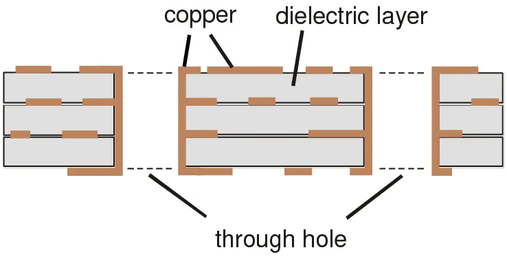
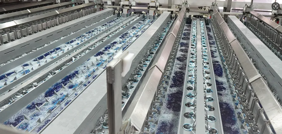
Copper plating in PCB manufacturing begins with electroless deposition to create a thin conductive seed layer on hole walls and surfaces, typically around 0.5 to 1 micrometer thick. This chemical process activates non-conductive substrates without external current, ensuring uniform coverage in through-holes and blind vias. Subsequent electrolytic plating applies bulk copper using an electric field, building thickness to the target weight through controlled current density and bath chemistry. Panel plating covers the entire board before patterning, while pattern plating focuses on traces for finer features, both critical for achieving precise PCB copper thickness. Factory monitoring of plating parameters prevents voids or overplating, which compromise interlayer adhesion. Variations in plating uniformity directly affect final copper weight tolerance, often held to plus or minus 10 percent in production.
Heavier copper builds demand extended plating times and higher current densities, increasing risks of dendritic growth or hydrogen embrittlement. Standards like IPC-A-600 define acceptability criteria for plating thickness and surface finish post-etching. Engineers must account for etch-back during pattern definition, as it reduces effective thickness by 20 to 30 percent depending on the process. This interplay between starting foil and plated copper dictates the final conductor profile, influencing downstream steps like solder mask application.
Impact on Current Carrying Capacity
Current carrying capacity in copper PCBs scales with copper thickness and trace width, as thicker conductors offer larger cross-sectional areas for electron flow. Per IPC-2221 guidelines, engineers calculate allowable current based on temperature rise limits, typically 10 to 30 degrees Celsius above ambient for reliable operation. Wider traces or heavier copper mitigate I2R losses, preventing hotspots that degrade insulation or components. In power distribution layers, 2 oz/ft2 or higher enables currents exceeding those of standard 1 oz/ft2 designs without excessive heating. Factory testing verifies these capacities through thermal imaging during qualification runs.
Heavier copper also improves voltage drop margins over long traces, essential for automotive or industrial controls. However, increased mass raises thermal expansion mismatches with dielectrics, potentially causing delamination under thermal stress. Design tools incorporate IPC-2221 charts to predict performance, ensuring traces meet derating factors for enclosed environments.
Effects on Impedance Control and Signal Integrity
Impedance control with copper weight becomes challenging as thickness variations alter characteristic impedance in transmission lines. Thicker copper lowers impedance due to increased conductor volume, requiring dielectric adjustments to maintain 50 or 100 ohm targets. For high-speed signals, even small deviations in PCB copper thickness shift return loss or crosstalk margins. Factory processes employ precise etching to control trace geometry, compensating for copper weight differences across layers. Simulations predict these effects, guiding stackup definitions for consistent impedance profiles.
In multilayer boards, asymmetric copper weights between signal and plane layers exacerbate skew, demanding balanced designs. Standards emphasize minimum thickness tolerances to support impedance verification post-fabrication.
Mechanical and Thermal Considerations in Heavy Copper Designs
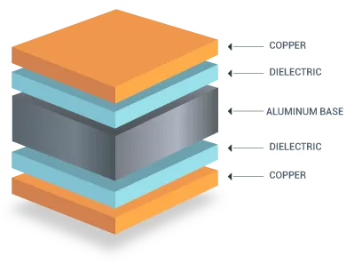
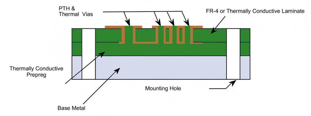
Heavy copper PCB design introduces unique challenges, defined as weights exceeding 3 oz/ft2, often up to 6 oz/ft2 or more for power applications. Thicker foils increase board rigidity but heighten warpage risks during lamination due to greater CTE differentials with FR-4 cores. Factories mitigate this through sequential lamination, building thicker sections incrementally to control bow and twist below 0.75 percent. Enhanced press cycles with higher pressures ensure void-free bonding under heavy copper stresses.
Thermal performance benefits from higher dissipation capacity, as thicker copper spreads heat more effectively across planes. However, uneven plating can create stress concentrations, leading to microcracks in vias. Engineers specify heavy copper strategically, pairing it with thermal vias and thicker cores for optimal heat paths.
Best Practices for Selecting and Implementing Copper Weight
Start with application analysis to determine minimum copper weight based on peak currents and frequency requirements. Use IPC-2221 for external trace capacities and derate for internals by 50 percent due to poorer convection. Collaborate with fabricators early to confirm plating capabilities, as heavy copper demands specialized racks and chemistry replenishment. Specify finished copper thickness in fabrication drawings, accounting for etch factor in trace width calculations.
For impedance-sensitive designs, model stackups with target copper weights and validate with TDR measurements. Employ step-down plating for hybrids, transitioning from heavy power layers to lighter signals. Post-etch inspections per IPC-A-600 ensure minimum thickness compliance, rejecting boards with underplated features.
In heavy copper PCB design, widen clearances to 2 mils per oz/ft2 beyond standard to prevent shorts during etching. Reinforce vias with plated thicknesses exceeding 25 micrometers and consider filled vias for high-current paths. These practices enhance yield and longevity in demanding production environments.
Troubleshooting Common Issues with Copper Weight Variations
Uneven copper thickness often manifests as impedance mismatches or hot spots during testing. Root causes include inconsistent plating currents or depleted baths, detectable via cross-section analysis. Factories adjust rectifier settings and analyze hull cells to maintain uniformity. Overetched heavy copper traces narrow excessively, reducing current carrying capacity; compensate by specifying wider artwork.
Warpage in heavy copper boards arises from asymmetric stacks; symmetrize layers or use constrained cores. Thermal cycling tests reveal delamination risks, prompting adhesion promoters in plating pre-treatments.
Conclusion
Mastering copper weight optimizes PCB performance across electrical, thermal, and mechanical domains. From copper plating PCB processes to heavy copper PCB design considerations, informed choices aligned with standards like IPC-2221 and IPC-6012 ensure robust outcomes. Electric engineers benefit from factory-driven insights, balancing thickness for current carrying capacity copper PCB needs while controlling impedance. Prioritizing precise specifications minimizes risks and enhances reliability in production. Future designs will leverage advancing plating techniques for even heavier coppers in power-dense applications.
FAQs
Q1: What is the standard PCB copper thickness for most applications?
A1: The standard PCB copper thickness is 1 oz/ft2, equivalent to about 35 micrometers finished, suitable for general signal and moderate power needs. This weight balances cost, etchability, and performance in multilayer boards. Factories achieve it via 0.5 oz starting foil plus plating buildup. Deviations require design adjustments for impedance control copper weight consistency.
Q2: How does copper thickness affect current carrying capacity in copper PCBs?
A2: Thicker copper increases cross-sectional area, boosting current carrying capacity copper PCB per IPC-2221 guidelines. For a 10-degree Celsius rise, capacity roughly doubles from 1 oz/ft2 to 2 oz/ft2 for equivalent widths. Engineers calculate using trace width and allowable ΔT. Heavier weights excel in power layers but demand wider spacings.
Q3: What challenges arise in heavy copper PCB design?
A3: Heavy copper PCB design, above 3 oz/ft2, complicates etching uniformity and increases warpage from CTE mismatches. Vias require thicker plating for reliability, and stackups need symmetry. Factories use extended cycles for plating. Benefits include superior thermal management for high currents.
Q4: How does copper weight influence impedance control?
A4: Copper weight impacts impedance control copper weight by altering conductor dimensions; thicker foils lower characteristic impedance in microstrips. Compensate with thinner dielectrics or wider traces. Simulations guide stackups. Fabrication tolerances ensure post-etch compliance.
References
IPC-2221B — Generic Standard on Printed Board Design. IPC, 2012
IPC-6012E — Qualification and Performance Specification for Rigid Printed Boards. IPC, 2015
IPC-A-600K — Acceptability of Printed Boards. IPC, 2020