Introduction
In the competitive landscape of electronics development, electric engineers face mounting pressures to deliver high-performance designs while managing budgets effectively. PCB manufacturing costs can quickly escalate due to complex designs, premium materials, and inefficient assembly processes, impacting overall project viability. Achieving cheap PCB manufacturing requires strategic decisions that prioritize pcb cost reduction without compromising reliability or functionality. This article outlines 10 proven ways to lower expenses in pcb design cost, pcb materials cost, and low cost PCB assembly, drawing from factory-floor best practices. By focusing on manufacturability and standardization, engineers can maintain adherence to industry benchmarks while optimizing expenditures. These approaches enable scalable production suitable for prototypes through high-volume runs.
Why PCB Cost Reduction Matters for Electric Engineers
PCB costs encompass design iterations, raw materials, fabrication, assembly, and testing, each influenced by engineering choices early in the process. For electric engineers, uncontrolled costs delay time-to-market and strain resources, particularly in iterative development cycles. Effective pcb cost reduction preserves signal integrity, thermal performance, and mechanical stability essential for applications like power electronics or control systems. Factory insights reveal that non-optimal designs lead to higher scrap rates and rework, amplifying expenses. Aligning with standards such as IPC-A-600 ensures quality remains intact during cost-saving measures. Ultimately, these strategies empower engineers to balance innovation with economic realities.
10 Ways to Reduce Your PCB Costs Without Sacrificing Quality
1. Embrace Design for Manufacturability (DFM) Principles
Incorporating DFM from the outset minimizes fabrication challenges and associated fees. Engineers should specify trace widths and spacings that align with standard tooling capabilities, avoiding overly fine features that demand specialized equipment. This approach reduces setup times and defect risks during etching and plating stages. By reviewing layouts against common process limits, designs become more predictable in production. Factory experience shows DFM streamlines workflows, contributing to overall pcb cost reduction. Quality stays high as these practices prevent issues like shorts or opens.
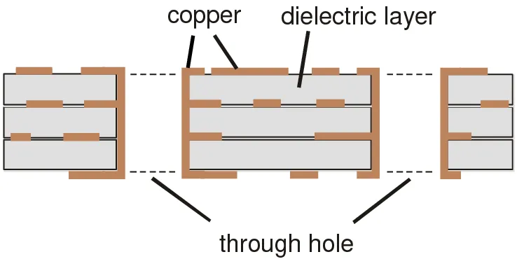
2. Minimize the Number of PCB Layers
Fewer layers directly lower material usage and processing complexity in multilayer boards. Electric engineers can consolidate routing by optimizing signal paths and ground planes, often achieving functionality with two or four layers instead of six or more. This reduces lamination cycles, drill hits, and registration challenges. Standard symmetric stackups further simplify pressing and baking steps. While high-density interconnects may require more layers, many designs permit reduction without performance loss. Resulting savings in fabrication make this a cornerstone of cheap PCB manufacturing.
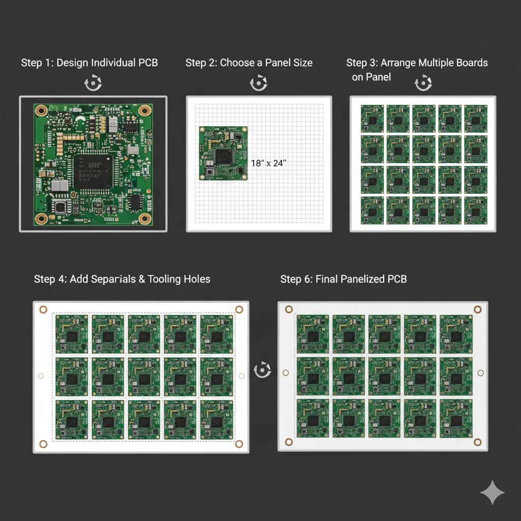
3. Optimize Board Size and Utilize Panelization
Designing boards to fit standard panel dimensions maximizes material yield and cuts per-unit costs, especially for low volumes. Engineers should aim for compact footprints that tile efficiently on production panels, reducing edge waste. Panelization also accelerates throughput by allowing batch processing of multiples. Consideration of scoring or tab routing ensures clean separation post-fabrication. This method maintains mechanical integrity while slashing pcb materials cost. Factories report significant efficiency gains from well-paneled jobs.
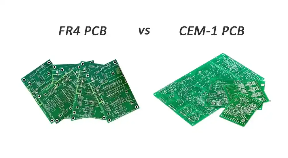
4. Select Standard and Cost-Effective Base Materials
Standard FR-4 laminates offer a reliable balance of performance and affordability for most applications under 1 GHz. Engineers avoid exotic high-Tg or low-loss materials unless thermal or frequency demands necessitate them, as these inflate pcb materials cost substantially. Verifying dielectric constants and thicknesses against application needs ensures no over-specification. Copper weights like 1 oz/ft2 suffice for many power designs, minimizing plating expenses. Adherence to qualification specs preserves reliability. This choice supports cheap PCB manufacturing across prototypes and production.
5. Standardize Drill Sizes and Reduce Via Counts
Using common drill diameters, such as 0.3 mm or larger, leverages existing tooling libraries and avoids custom bit charges. Engineers can minimize vias by strategic routing and fanouts, favoring through-hole over blind or buried where possible. Larger annular rings enhance yield during plating. This reduces machine time and inspection efforts. Factory data indicates fewer unique drills correlate with lower setup fees. Quality benefits from reduced aspect ratios, aligning with IPC-6012 guidelines for rigid boards.
6. Choose Economical Surface Finishes
Hot Air Solder Leveling (HASL) or Organic Solderability Preservative (OSP) provides cost-effective protection compared to premium options like ENIG for non-fine-pitch needs. Engineers select finishes based on shelf life, solderability, and assembly methods, ensuring compatibility with reflow profiles. Lead-free HASL suits many electric designs without barrel fill issues. This decision impacts solder joint reliability positively when matched to process controls. Savings accrue from simpler application steps. Low cost PCB assembly improves as these finishes support standard wave or reflow soldering.
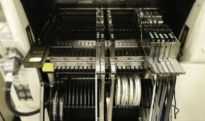
7. Standardize Components for Assembly Efficiency
Opting for readily available, standard-package components reduces procurement premiums and assembly handling times. Electric engineers prioritize 0805 or 1206 passives over odd sizes, facilitating pick-and-place automation. Unified orientations minimize feeder changes and programming efforts. Bill of Materials (BOM) simplification cuts kitting costs. This strategy enhances low cost PCB assembly without altering circuit performance. Factories achieve higher throughput, lowering per-board fees.
8. Optimize Component Placement and Routing for DFA
Design for Assembly (DFA) involves grouping components by type and aligning them for unidirectional placement paths. Engineers space parts to avoid shadowing during stencil printing and reflow. Fiducial marks in corners aid machine vision without excess proliferation. Balanced copper distribution prevents warpage. These practices reduce solder defects per J-STD-001 requirements for soldered assemblies. Pcb cost reduction follows from fewer rejects and faster cycles.
9. Streamline Solder Mask and Silkscreen Layers
Applying solder mask only where needed, with standard green LPI, avoids custom colors or thicknesses that raise costs. Engineers limit silkscreen to essential markings like polarities and references, using smaller fonts for density. Clear apertures over pads ensure clean soldering. This conserves material and simplifies exposure steps. No compromise on insulation or identification occurs. Integration into the fabrication flow supports cheap PCB manufacturing.
10. Enhance Documentation and Gerber Accuracy
Providing complete, error-free Gerber files and fabrication drawings eliminates iterations and rush fees. Engineers include drill files, panel specs, and stackup details upfront. Layer naming conventions prevent mix-ups. Pre-flight checks catch issues like missing stops or apertures. Factories process accurate packages swiftly, aiding pcb cost reduction. Quality upholds as precise instructions align with standards like IPC-A-600.
Conclusion
Implementing these 10 strategies empowers electric engineers to achieve substantial pcb cost reduction across design, materials, fabrication, and assembly phases. From DFM adherence to standardized features, each method targets inefficiencies while upholding performance and reliability. Factory-driven insights confirm that proactive choices yield the best outcomes in cheap PCB manufacturing. Engineers balancing complexity with simplicity position projects for success. Regular reviews against evolving needs sustain long-term savings. Prioritize these practices for optimal results.
FAQs
Q1: How can DFM principles contribute to pcb cost reduction?
A1: DFM ensures designs match standard fabrication capabilities, reducing custom tooling and rework. Engineers optimize traces, vias, and spacings early, aligning with process limits. This lowers setup times and scrap rates without affecting functionality. Factories process DFM-compliant boards faster, directly impacting cheap PCB manufacturing costs. Overall, it streamlines from prototype to volume production.
Q2: What role do materials play in pcb materials cost savings?
A2: Standard FR-4 suits most electric engineering applications, offering low cost without sacrificing dielectric properties. Avoid high-spec alternatives unless required for heat or speed. Verify thicknesses and copper weights against needs to prevent overbuild. This keeps expenses down while meeting performance specs. Proper selection enhances manufacturability.
Q3: Why is panelization key for low cost PCB assembly?
A3: Panelization maximizes panel utilization, cutting per-board material and handling fees for small runs. Designs tile efficiently with routing tabs for separation. It boosts throughput in assembly lines via batch processing. Engineers gain economies without quality loss. Ideal for scaling prototypes.
Q4: How does component standardization aid pcb design cost control?
A4: Standard packages enable automated assembly, reducing programming and feeder costs. Unified sourcing stabilizes pricing. Electric engineers select common values for passives and ICs. This minimizes BOM complexity and lead times. Supports reliable low cost PCB assembly per industry practices.
References
IPC-A-600K - Acceptability of Printed Boards. IPC, 2020
IPC-6012E - Qualification and Performance Specification for Rigid Printed Boards. IPC, 2017
J-STD-001H - Requirements for Soldered Electrical and Electronic Assemblies. IPC/JEDEC, 2018