Introduction
Sequential build-up (SBU) PCBs represent a cornerstone technology for achieving high-density interconnects in compact electronic devices. These boards support advanced features like blind vias, buried vias, and microvias, enabling tighter routing and smaller footprints essential for applications in telecommunications, automotive electronics, and consumer gadgets. However, the iterative lamination processes involved in SBU fabrication often drive up manufacturing expenses due to specialized materials, precision drilling, and multiple plating cycles. Electric engineers seeking sequential build-up PCB cost optimization must balance performance demands with practical design choices that minimize waste and streamline production. This article delves into proven strategies, drawing from factory-driven insights to guide material selection, layer management, and process efficiency. By implementing these approaches, designers can deliver reliable boards without prohibitive costs.
What Is Sequential Build-Up PCB and Why It Matters
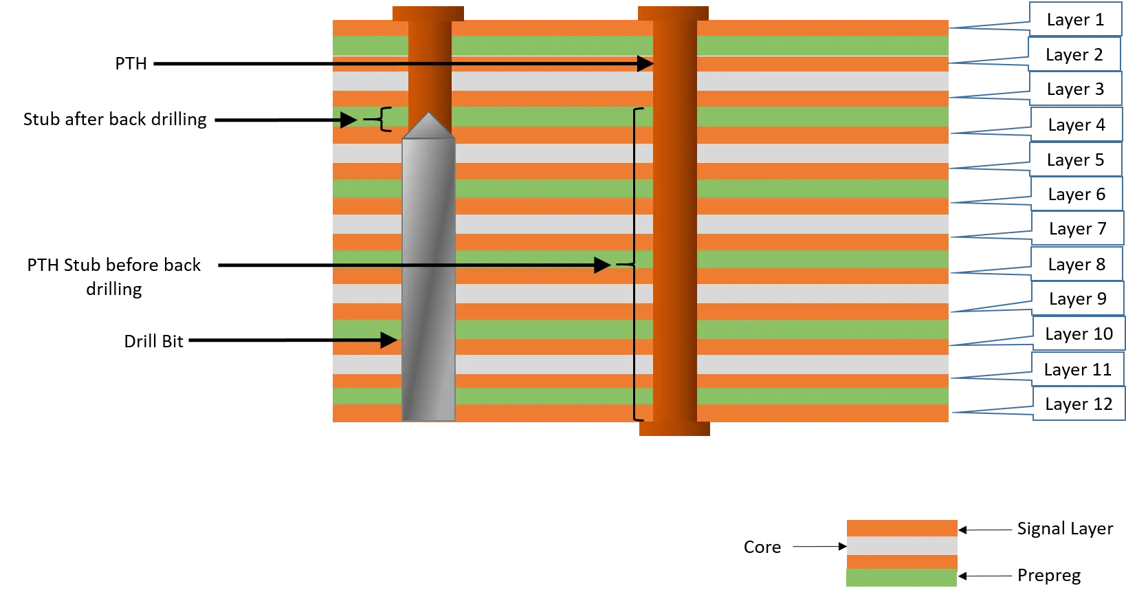
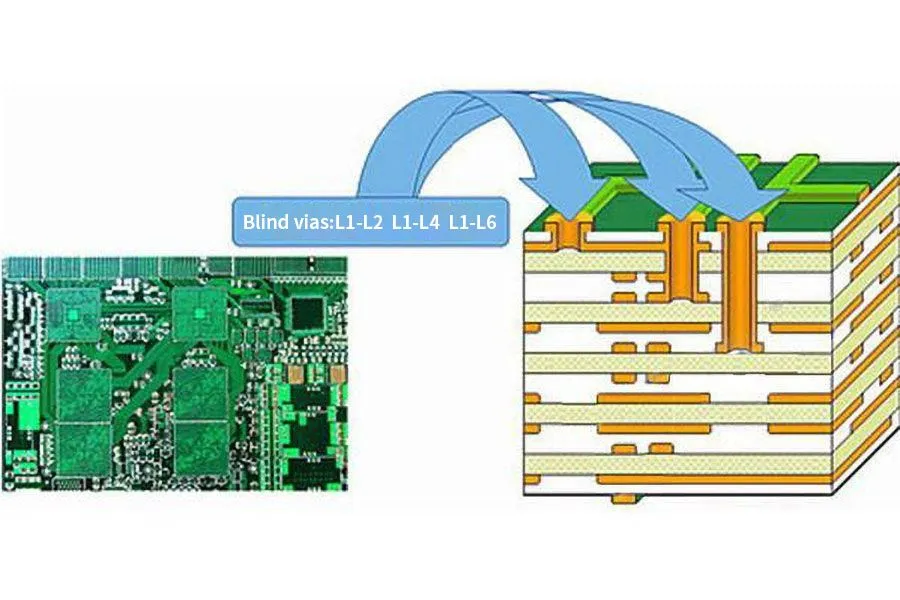
Sequential build-up PCB fabrication starts with a central core layer, typically a standard multilayer substrate, around which additional thin dielectric and copper layers are sequentially laminated. Each build-up cycle involves laser drilling for vias, photosensitive dielectric application, patterning, and electroplating to form interconnects. This method contrasts with traditional all-at-once lamination by allowing precise control over via stacking and layer sequencing, which is critical for high-density designs. The resulting boards, often classified as high-density interconnect (HDI) types, support finer pitch components and reduced signal path lengths, improving electrical performance.
In industry contexts, SBU PCBs matter because they enable miniaturization without compromising signal integrity or thermal management. Electric engineers encounter them in designs where space constraints demand via-in-pad or stacked microvias, such as in 5G modules or medical wearables. Yet, the complexity translates to higher costs from yield risks like via misalignment or warpage during repeated thermal cycles. Effective sequential build-up PCB cost optimization becomes vital for mid-volume production, ensuring competitiveness while adhering to reliability standards like IPC-2226 for HDI design rules.
Technical Principles Driving SBU PCB Costs
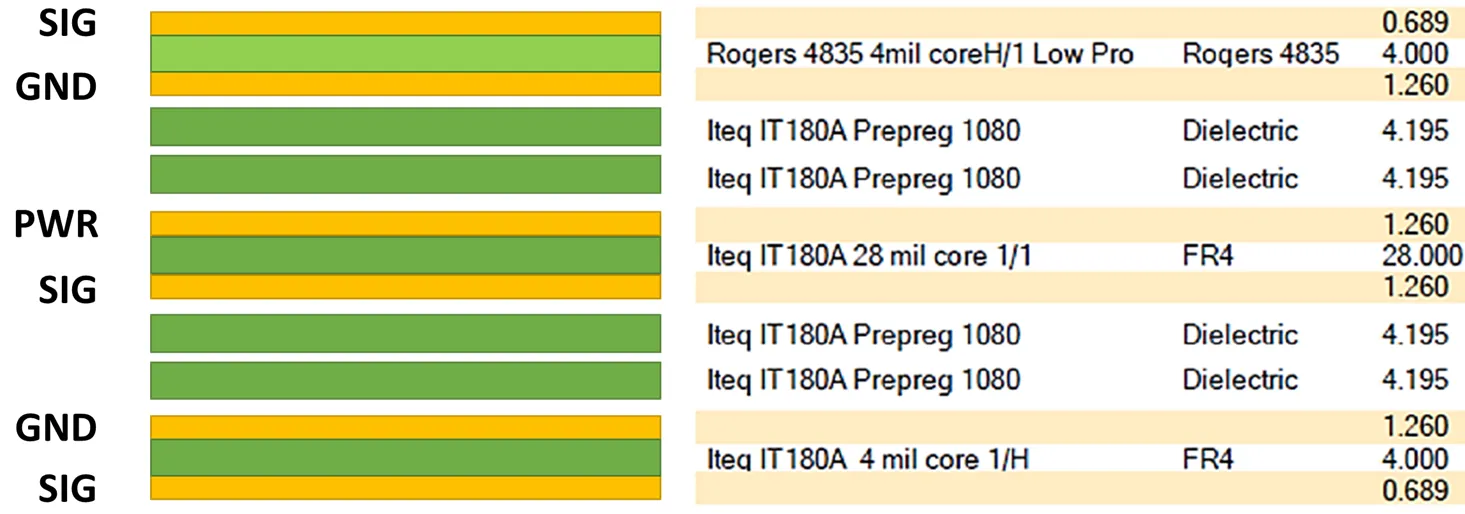
The cost structure of SBU PCBs stems from the multi-step build-up process, where each additional layer incurs expenses in material deposition, via formation, and quality inspection. Laser ablation for microvias requires UV or CO2 lasers to etch precise holes in thin dielectrics, followed by desmear and plating, which multiplies handling and equipment time. Material properties play a key role; dielectrics with low coefficient of thermal expansion (CTE) prevent warpage from copper-dielectric mismatches during lamination presses at elevated temperatures. Factory experience shows that asymmetric stackups exacerbate bow and twist, leading to scrap rates that inflate per-unit costs.
Via reliability adds another layer of expense, as stacked or staggered microvias must withstand cyclic thermal stress without cracking, per guidelines in IPC-2226. Plating cycles for electroless copper and electroplating consume chemicals and generate waste, with filled vias offering robustness but at higher material use. Registration accuracy across build-ups demands advanced alignment systems, as tolerances tighten to 50 microns or less for inner layers. Understanding these mechanisms allows engineers to target interventions that reduce process iterations without sacrificing density.
Strategies for Sequential Build-Up PCB Cost Optimization
Sequential Build-Up PCB Material Selection Cost
Material choices directly influence sequential build-up PCB material selection cost, as high-performance dielectrics dominate expenses in HDI builds. Opt for resin-coated copper (RCC) or low-flow prepregs that support laser drilling without excessive smear, reducing post-processing steps. These materials balance cost with properties like glass transition temperature (Tg) above 170°C for lamination stability and dielectric constant (Dk) suited to signal speeds. Factory insights reveal that selecting thinner dielectrics, around 50-100 microns, cuts volume usage while maintaining via aspect ratios under 1:1 per IPC-2226 recommendations.
Avoid over-specifying for low-loss resins unless RF performance mandates it; standard FR-4 compatible build-up sheets suffice for many digital designs. Symmetric material pairing on both sides of the core minimizes CTE-induced warpage, improving yields. Procurement teams benefit from volume buying of qualified lots, but engineers should verify compatibility through thermal simulations early. This targeted selection can lower material outlay by focusing on manufacturable grades that meet performance without premium pricing.
Sequential Build-Up PCB Layer Count Cost
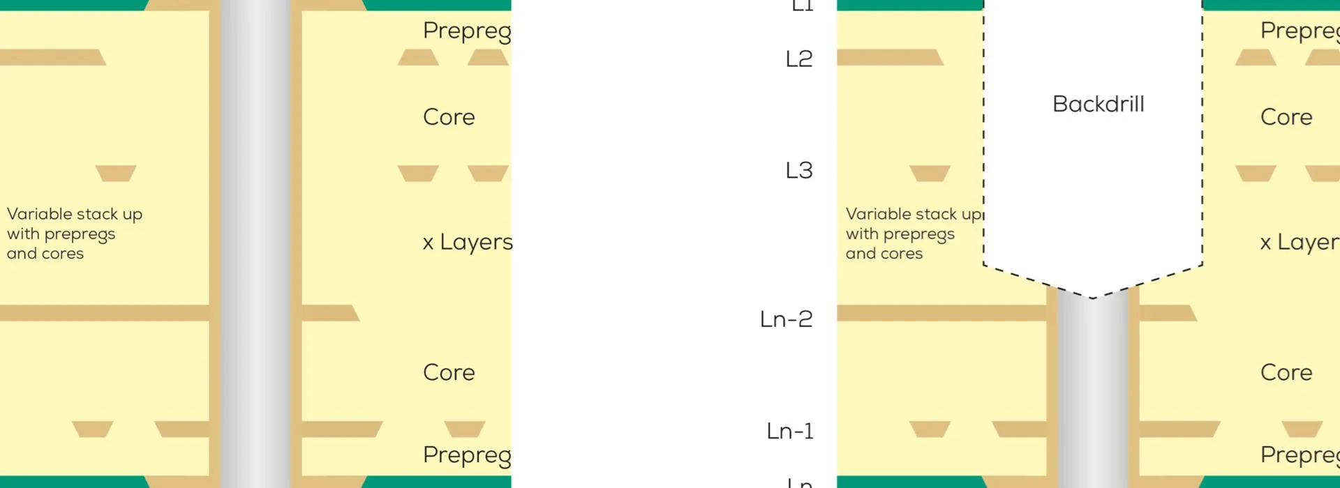
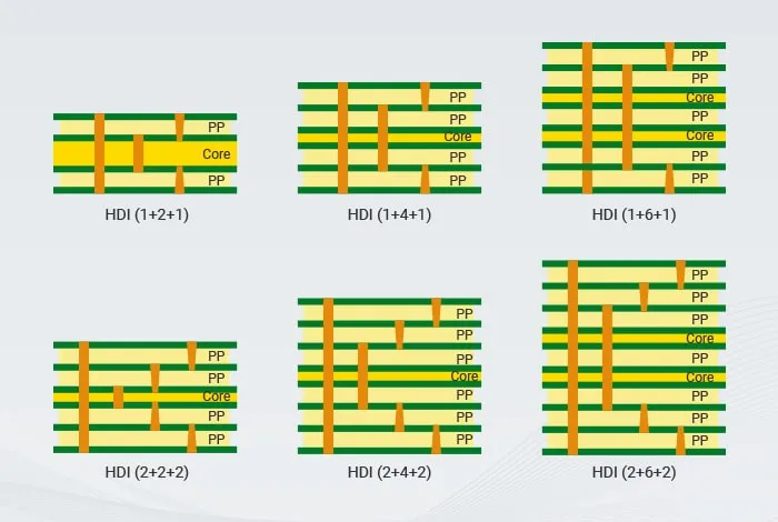
Layer count profoundly impacts sequential build-up PCB layer count cost, as each build-up pair doubles lamination, drilling, and plating operations. Engineers should default to minimal configurations like 1+N+1, where one HDI layer builds on each side of an N-layer core, reserving 2+N+2 or higher for extreme densities. Staggered vias, alternating positions between layers, reduce plating depth and cycle time compared to fully stacked arrangements. Design reviews often uncover opportunities to merge ground planes or reroute signals on core layers, eliminating unnecessary outer build-ups.
Adhering to IPC-2226 via capture and escape pad rules ensures reliability while allowing larger, cheaper vias. Simulate routing density upfront to confirm if core layers handle most traces, pushing high-speed nets to outer layers only as needed. Factory data underscores that halving build-up steps correlates with proportional cost drops, provided signal integrity holds via controlled impedance stackups. This optimization demands iterative layout but yields substantial savings in production scaling.
Sequential Build-Up PCB Manufacturing Process Cost
Streamlining the sequential build-up PCB manufacturing process cost involves design-for-manufacturability (DFM) principles that align with factory capabilities. Standardize via diameters to 100-150 microns, avoiding sub-75 micron sizes that require specialized lasers and raise defect risks. Panelize boards efficiently, using 18x24 inch arrays with v-scoring for depaneling, to maximize substrate utilization and spread setup costs. Sequential lamination benefits from symmetric stackups, which control warpage below 0.75% as per IPC-A-600 acceptability criteria, minimizing rework.
Integrate filled vias selectively for high-stress locations, as they enable thinner subsequent dielectrics but consolidate plating in fewer baths. Reduce cycle times by grouping drill patterns and using progressive lamination, where outer layers finalize after inner cures. Quality gates like automated optical inspection (AOI) after each build-up catch issues early, preserving yields. These process tweaks, rooted in standard workflows, compound savings across volume runs.
Best Practices for Implementation
Implement sequential build-up PCB cost optimization through cross-functional reviews involving design, fabrication, and procurement. Start with stackup planning software to model thermal and mechanical stresses, ensuring CTE matching across materials. Prototype single-build iterations to validate via reliability before full SBU commitment. Collaborate with manufacturers on capability matrices, confirming support for your chosen via types and layer configs.
Document DFM checklists covering pad clearances, annular ring sizes, and aspect ratios per IPC-2226. Monitor key metrics like first-pass yield and cycle time during pilot runs, iterating on pain points. For scalability, qualify processes under IPC-6012 performance specs to assure consistency.
Conclusion
Sequential build-up PCBs offer unmatched density for demanding applications, but unchecked complexity erodes cost-effectiveness. By prioritizing sequential build-up PCB material selection cost through efficient dielectrics, managing sequential build-up PCB layer count cost via minimal builds, and refining sequential build-up PCB manufacturing process cost with DFM, engineers unlock affordable high-performance boards. Standards like IPC-2226 and IPC-A-600 provide the guardrails for reliable execution. These strategies not only trim expenses but enhance yield and speed-to-market, empowering competitive designs in a density-driven market.
FAQs
Q1: How does sequential build-up PCB material selection cost influence overall fabrication budgets?
A1: Selecting cost-effective dielectrics like RCC or standard prepregs reduces raw material expenses while supporting laser via formation. Prioritize materials with matched CTE to the core for warpage control, aligning with factory lamination presses. Thinner layers cut usage without violating IPC-2226 rules, directly lowering per-board costs in volume production. This approach maintains HDI performance for electric engineers focused on balanced budgets.
Q2: What role does layer count play in sequential build-up PCB layer count cost optimization?
A2: Minimizing build-up layers, such as using 1+N+1 configurations, halves lamination and plating cycles compared to advanced stacks. Route high-density nets strategically on core layers to avoid extra outer builds. Staggered vias further streamline processes per IPC-2226 guidelines. Factory-driven designs prove this yields significant savings without density trade-offs.
Q3: What are key tactics for sequential build-up PCB manufacturing process cost reduction?
A3: Panelization and standard via sizes optimize material use and tooling. Symmetric stackups prevent warpage, boosting yields as inspected under IPC-A-600. Limit filled vias to critical spots and sequence laminations progressively. These DFM practices cut handling time and waste in HDI production lines.
Q4: Why is IPC-2226 essential for sequential build-up PCB cost optimization efforts?
A4: IPC-2226 outlines HDI design rules for microvias, pads, and stackups, ensuring manufacturability. Compliance avoids costly redesigns from via failures or registration errors. It guides layer minimization and material choices for efficient factories. Engineers rely on it for reliable, cost-controlled SBU implementations.
References
IPC-2226 — Design Standard for High Density Interconnects. IPC
IPC-A-600K — Acceptability of Printed Boards. IPC, 2020
IPC-6012E — Qualification and Performance Specification for Rigid Printed Boards. IPC, 2017