Introduction
V-scoring PCB depaneling stands as a cornerstone in high-volume electronics manufacturing, enabling efficient singulation of multiple boards from a single panel. This method involves creating precise V-shaped grooves along designated lines, allowing boards to be separated with minimal stress and equipment. For electric engineers designing panels for mass production, optimizing V-scoring directly impacts yield rates, assembly reliability, and overall production costs. Poorly executed V-scoring can lead to issues like microcracking, warpage, or delamination during separation, compromising board integrity. By understanding the interplay of design, tolerances, and depaneling processes, engineers can achieve superior V-cut PCB singulation outcomes. This article delves into the technical principles, best practices, and optimization strategies to ensure success.
What Is V-Scoring and Why Does It Matter?
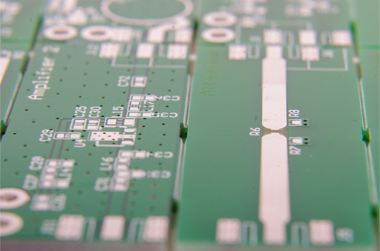
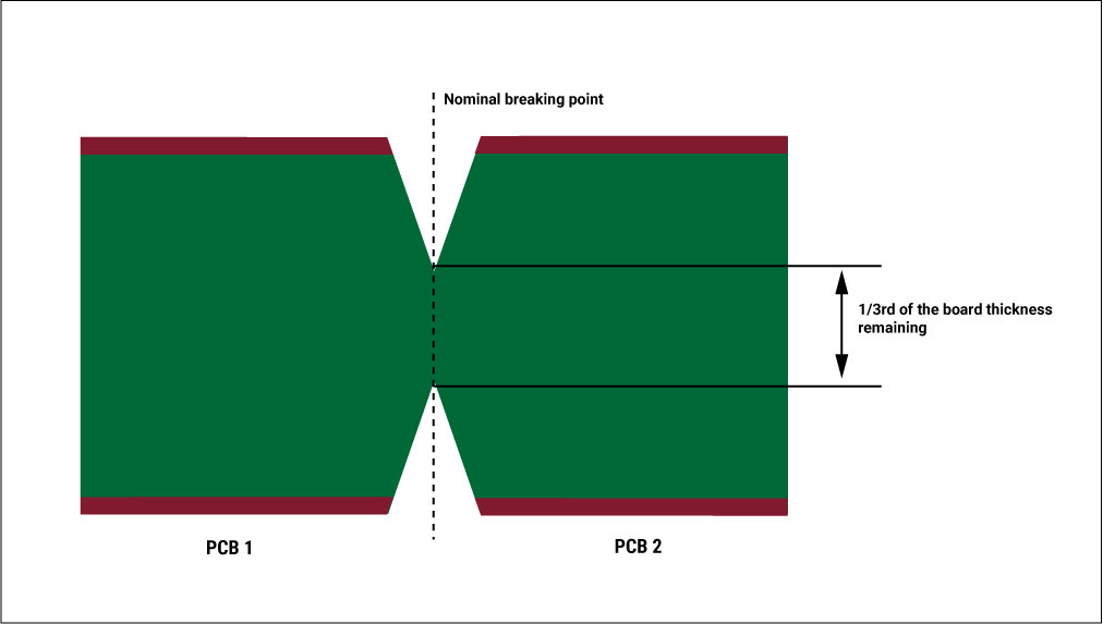
V-scoring, also known as V-cutting, is a mechanical depaneling preparation technique where trapezoidal grooves are machined into the top and bottom surfaces of a PCB panel along straight lines. These grooves meet at a thin residual web of material, typically one-third or more of the board thickness, which holds the individual boards together during fabrication and assembly. During final singulation, linear force snaps the web cleanly, separating boards without the need for complex tooling. This contrasts with routing or tab-based methods, which require more panel border space and can generate dust or burrs.
The relevance of V-scoring PCB depaneling lies in its scalability for rectangular or square panels in high-volume runs. It maximizes V-score material utilization by allowing tighter board spacing, often approaching zero millimeters between units, which reduces waste and lowers PCB depaneling costs compared to alternatives. For electric engineers, this method supports automated assembly lines where quick, repeatable singulation is essential. However, success hinges on adhering to V-score design rules to prevent stress concentrations that could propagate cracks into active circuitry. Industry standards like IPC-2221 provide foundational guidelines for these parameters, ensuring mechanical reliability aligns with electrical performance.
In practice, V-scoring excels for boards with straight edges and uniform thickness, typically starting from 1.0 mm upward. It minimizes material loss, boosting panel efficiency to high levels suitable for consumer electronics and automotive applications. Engineers must weigh it against board complexity; irregular shapes demand hybrid approaches.
Technical Principles of V-Scoring
The core mechanism of V-scoring revolves around controlled stress concentration at the groove apex. Grooves are typically formed at angles between 30 and 60 degrees using gang saws or specialized milling tools, penetrating partially from both sides to leave a uniform web. This geometry facilitates even distribution of bending stress during depaneling, where the panel is flexed until the web fractures along the score line. PCB depaneling stress arises primarily from tensile and shear forces at the web, potentially inducing microcracks if the residual material is too thin or uneven.
Material properties play a critical role; FR-4 laminates with standard glass transition temperatures exhibit predictable fracture behavior under these loads. Thicker boards distribute stress better, but thin flex-rigid hybrids may require shallower cuts to avoid warpage. IPC-6012E outlines qualification criteria for such features, emphasizing dimensional stability post-scoring. Misalignment in groove depth or angle amplifies localized strain, risking delamination at copper-layer interfaces.
V-scoring tolerances dictate manufacturing precision, encompassing groove width, depth variation, and positional accuracy relative to fiducials. Deviations beyond tight limits can shift stress profiles, leading to incomplete breaks or overshoot into adjacent traces. Engineers model these using finite element analysis to predict failure modes, correlating groove parameters with maximum allowable strain.
Environmental factors like panel bow or humidity absorption further influence mechanics. Pre-baked panels minimize moisture-induced swelling, preserving tolerance stacks. Overall, these principles underscore the need for integrated design-fabrication feedback loops.
V-Score Design Rules and Tolerances
Effective V-score design rules begin with panel layout optimization. Scores must run straight from edge to edge, perpendicular or parallel to board edges, on rectangular arrays only. Minimum board dimensions ensure stable handling, while maximum panel sizes align with V-scoring equipment capacities. Conductor clearances from score lines prevent exposure during groove formation, as specified in IPC standards for mechanical features.
Residual web thickness serves as the primary control parameter, scaled to board thickness to balance singulation ease and strength. Too thin a web invites premature cracking; too thick resists clean breaks. Tolerances on this dimension, often held to fine limits, directly affect PCB depaneling stress uniformity. Positional tolerances for groove alignment relative to board outlines maintain symmetry, crucial for automated depaneling.
Component placement rules prohibit tall or dense parts near scores to mitigate shock transmission. Vias and traces require offsets to avoid fracture propagation. These rules enhance V-score material utilization by enabling dense nesting without tabs or rails.
Designers iterate using panelization software to visualize stress hotspots. Compliance with IPC-A-600 acceptability criteria verifies post-scoring quality.
Practical Solutions and Best Practices for Optimization
Optimizing V-scoring starts with material selection; low-CTE laminates reduce warpage risks during thermal excursions. Panelization prioritizes maximal board count per sheet, leveraging V-scoring's zero-spacing advantage for superior material utilization. Hybrid scoring with jumps allows complex outlines while retaining straight-line efficiency.
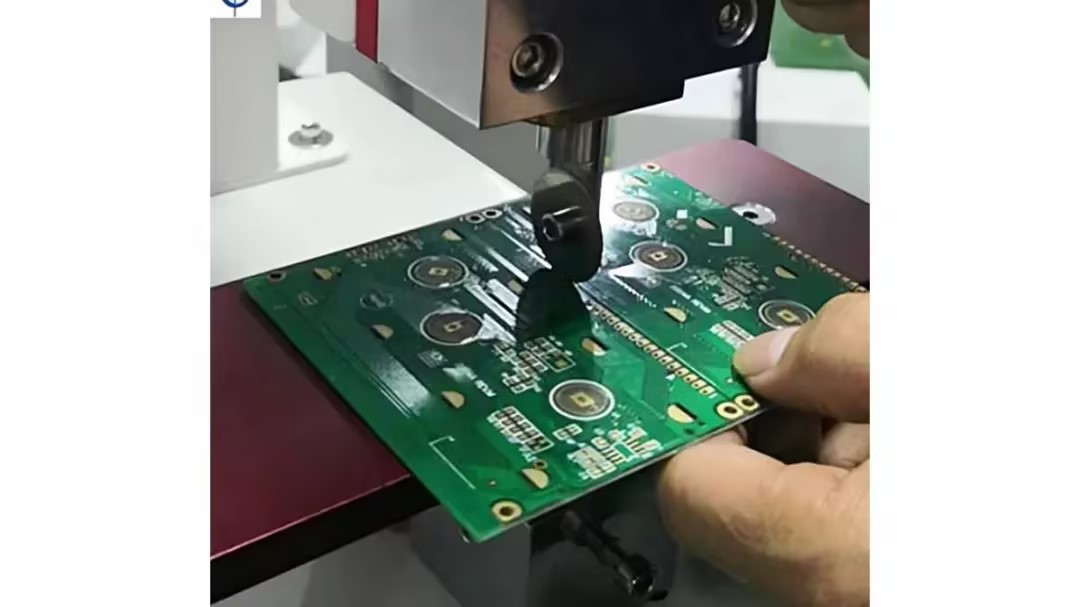
V-scoring equipment varies from manual snap tools for prototypes to automated linear depanelers for production. Selection factors include board thickness range, throughput, and stress monitoring capabilities. Low-force machines with adjustable blades minimize PCB depaneling stress, extending fixture life and yield.
Best practices include validation through strain gauge testing on sample panels. Maintain groove angles consistent across runs to control fracture energy. Post-depaneling inspections check for burrs or edge damage per IPC guidelines.
PCB depaneling cost optimization favors V-scoring for volumes over 1000 units, as setup is minimal and cycle times short. Track metrics like web break force and scrap rate to refine processes.
Troubleshooting Common V-Scoring Challenges
Engineers often encounter incomplete singulation from overly robust webs or thick boards. Solution: deepen grooves within tolerance or use assisted force. Excessive stress causing microcracks signals poor tolerances; recalibrate equipment and verify panel flatness.
Warpage post-depaneling traces to asymmetric scoring or bow; counter with symmetric dual-sided cuts and fixturing. Delamination near scores points to resin voids; inspect incoming laminates.
Case insight: A panel with dense BGA near scores failed reliability tests due to propagated cracks. Redesign shifted components 5 mm away, incorporating jump scores, yielding 99% first-pass success.
Conclusion
Mastering V-scoring PCB depaneling demands a holistic approach integrating design rules, precise tolerances, and equipment selection. By minimizing PCB depaneling stress and maximizing V-score material utilization, engineers unlock cost efficiencies and reliability gains. Adhering to standards like IPC-2221 and IPC-6012E ensures robust outcomes across production scales. Implement these strategies to elevate V-cut PCB singulation from routine to optimized excellence.
FAQs
Q1: What are the key V-score design rules for reliable PCB depaneling?
A1: V-score design rules emphasize straight-line grooves on rectangular panels, sufficient conductor offsets, and residual web thickness proportional to board height per IPC-2221. Panel layouts maximize density for material utilization while avoiding components near scores. Tolerances on groove depth and position prevent stress imbalances. Following these reduces risks in high-volume V-scoring PCB depaneling.
Q2: How does V-scoring tolerances impact depaneling stress?
A2: Tight V-scoring tolerances ensure uniform groove geometry, distributing bending stress evenly during singulation. Deviations amplify localized strains, risking cracks or warpage. Engineers monitor via prototypes to hold limits, optimizing for low-force breaks. This directly lowers PCB depaneling stress in production.
Q3: What factors influence PCB depaneling cost with V-scoring?
A3: V-scoring offers low setup and equipment costs, ideal for volume runs with minimal waste. Panel complexity and size affect machine time, while tolerances drive scrap. Choosing efficient V-scoring equipment and dense layouts cuts overall PCB depaneling cost significantly.
Q4: How to improve V-score material utilization in panel design?
A4: Prioritize zero-spacing arrays on rectangular boards, using continuous or jump V-cuts for flexibility. Avoid tabs to pack more units per panel. Validate layouts for depaneling feasibility, boosting efficiency in V-cut PCB singulation.
References
IPC-2221B — Generic Standard on Printed Board Design. IPC, 2003
IPC-6012E — Qualification and Performance Specification for Rigid Printed Boards. IPC, 2015
IPC-A-600K — Acceptability of Printed Boards. IPC, 2020


