What Exactly is a Multi-Layer PCB and Why Build One Yourself?
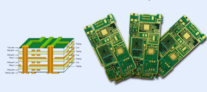
A multi-layer Printed Circuit Board (PCB) goes beyond the common double-sided design, incorporating more than two conductive copper layers, each separated by insulating material. These layers are carefully stacked and bonded into a single, compact board. Such sophisticated designs are indispensable for modern, complex electronic devices, enabling greater circuit density, superior signal integrity, and a significant reduction in electromagnetic interference. For the dedicated electronics hobbyist, undertaking the creation of a multi-layer PCB at home offers substantial benefits, including cost savings, accelerated prototyping cycles, and complete freedom to customize designs for unique project requirements.
The sequential build-up (SBU) method involves constructing the PCB layer by layer, meticulously aligning and bonding each one to ensure seamless functionality. While this process presents a degree of challenge, it is entirely achievable within a home workshop, provided one has the right tools, a methodical approach, and a good dose of patience. This comprehensive guide aims to demystify each stage, empowering you to successfully fabricate professional-quality multi-layer PCBs from your own workspace.
Advantages of DIY Multi-Layer PCBs for Hobbyists
● Significant Cost Reduction: Professional fabrication of multi-layer PCBs can be quite expensive, especially for small-batch runs. Doing it yourself offers considerable savings.
● Unrestricted Customization: Design boards precisely to your project's unique specifications, free from the limitations often imposed by standard manufacturing processes.
● Valuable Skill Development: Gaining proficiency in advanced PCB etching, lamination, and via creation techniques at home provides invaluable expertise for future endeavors.
● Accelerated Prototyping: Eliminate the weeks-long waiting periods associated with external manufacturers, allowing you to test and iterate on your designs in just a few days.
Essential Tools and Materials for Home Multi-Layer PCB Production
Embarking on the journey of sequential build-up PCB fabrication at home requires a specific set of tools and materials. Having all necessary items prepared in advance will not only streamline your workflow but also help minimize potential errors throughout the intricate process.
Key Components and Equipment
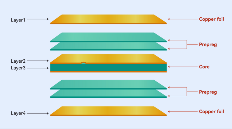
● Copper-Clad Laminates: Acquire thin, double-sided copper boards for each internal and external layer of your PCB. Common thicknesses might range from 0.8mm to 1.6mm.
● Prepreg Sheets: These are insulating sheets of partially cured fiberglass-epoxy resin, crucial for bonding the copper layers together under heat and pressure.
● Etching Agent: Prepare a suitable solution such as ferric chloride or sodium persulfate, essential for selectively removing copper during the etching process.
● Design Transfer Medium: Choose between toner transfer paper (used with a laser printer) or photoresist film, which will carry your circuit patterns onto the copper.
● Lamination Tool: An office laminator or even a household iron can be repurposed for transferring toner designs or assisting with basic PCB lamination.
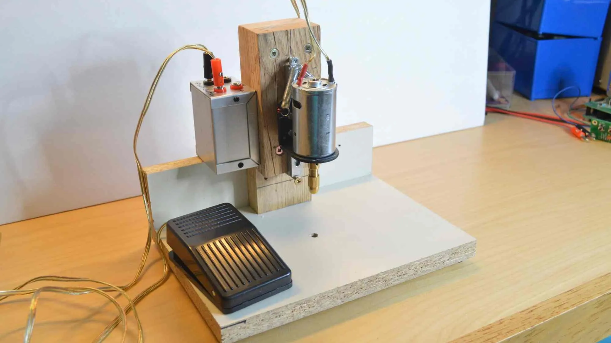
● Precision Drilling Setup: A drill press equipped with very small drill bits (e.g., 0.3mm to 1mm) is vital for accurately creating vias.
● Via Interconnection: Small copper rivets or specialized conductive ink are needed to establish electrical connections through drilled vias between layers.
● Heat & Pressure Apparatus: A heat press or even a modified home oven can serve to bond the layers together during the sequential build-up process.
● Safety Gear: Always wear protective gloves and goggles, and ensure your workspace is well-ventilated when handling chemicals.
● PCB Design Software: Utilize freely available CAD tools to design your circuit layouts and prepare them for printing.
Maintaining a clean and organized workspace is paramount to prevent contamination and ensure precise alignment during the multi-layer construction.
A Step-by-Step Guide to Crafting Your Own Multi-Layer PCB
Let's meticulously detail the sequential process of constructing a multi-layer PCB in your home workshop. Adhering to these steps carefully will yield the best results for your DIY project.
Step 1: Design and Layout Your Multi-Layer PCB
Begin by meticulously designing each individual layer of your PCB using appropriate software. Carefully plan the positioning of components, the routing of traces, and the location of vias to guarantee perfect alignment when the layers are stacked. For a typical four-layer board, you might designate:
● Top Layer: Dedicated to signals and component placement.
● Inner Layer 1: Often serves as a ground plane.
● Inner Layer 2: Commonly used as a power plane.
● Bottom Layer: For additional signals or components.
Export each layer’s design as a high-resolution image or PDF suitable for printing. Crucially, ensure that all vias (the holes connecting different layers) are clearly marked on your design, as their accurate placement is fundamental to the board's functionality.
Step 2: Prepare and Etch Individual Layers
With your designs ready, the next phase involves transferring these patterns onto the copper-clad boards and then selectively etching the copper.
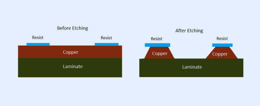
● Print Your Design: Using a laser printer, print each layer's circuit pattern onto toner transfer paper or photoresist film. Remember to mirror the image if you are using the toner transfer method to ensure correct orientation on the copper.
● Transfer the Pattern: Position the printed design face-down onto a thoroughly cleaned copper-clad board. Apply heat and even pressure with a laminator or an iron for about 2-3 minutes to transfer the toner effectively onto the copper surface.
● Etch the Copper: Submerge the board into your prepared etching solution (e.g., ferric chloride diluted 1:3 with water) for approximately 10-20 minutes. Gentle agitation can help accelerate the etching process. The unprotected copper will dissolve, leaving behind your circuit traces. After etching, rinse the board thoroughly with water and then use acetone to remove the remaining toner.
Repeat this precise process for every layer that will constitute your multi-layer PCB. Pay close attention to alignment marks to confirm that all layers will stack together perfectly.
Step 3: Drill Vias for Inter-Layer Connectivity
Creating vias at home is a vital step for establishing electrical connections between the various layers of your PCB. Vias are small, precisely drilled holes that will later be made conductive to allow electricity to pass from one layer to another.
● Mark Via Positions: Refer to your digital design to accurately mark the exact locations where vias need to be drilled on each etched layer.
● Precision Drilling: Utilize a drill press with a fine drill bit (typically between 0.3mm and 0.8mm) to ensure high precision. If possible, temporarily align a few layers and drill through them simultaneously to guarantee that the holes correspond exactly across the stack.
● Establish Via Connections: For a straightforward DIY approach, insert tiny copper rivets into the drilled holes or meticulously fill them with conductive ink to create the necessary electrical pathways. While more advanced, electroplating can offer superior reliability if you have access to the specialized equipment.
Before proceeding to the lamination stage, ensure all vias are clean and completely free of any debris that could impede conductivity.
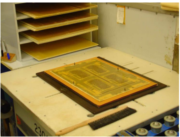
Step 4: Laminate Layers Using the Sequential Build-Up Method
PCB lamination for hobbyists involves carefully bonding the individually etched layers together using insulating prepreg sheets, under controlled heat and pressure. The sequential build-up method means you bond one layer assembly at a time, allowing for verification at each stage before adding the next.
● Prepare Your Stack: Arrange your etched copper boards with prepreg sheets placed between each copper layer. Prepreg is a semi-cured epoxy-fiberglass material that solidifies when subjected to heat. Typically, 1-2 sheets (each around 0.1mm thick) are used per gap to ensure adequate insulation.
● Achieve Perfect Alignment: Employ alignment pins or precisely marked registration points to ensure that all traces and vias from one layer perfectly line up with the next. Even slight misalignment can critically compromise connectivity.
● Bond with Heat and Pressure: Carefully place the assembled stack into a heat press or a DIY setup (such as between heavy metal plates within an oven). Apply consistent heat, typically between 170-180°C, and even pressure (around 50-100 psi, if measurable) for 1-2 hours. This process fully cures the prepreg, permanently bonding the layers into a single, robust circuit board.
● Controlled Cooling: Allow the laminated board to cool down slowly while still under pressure. This prevents warping and ensures a stable, flat final product.
After each lamination step, meticulously inspect the board for any signs of air bubbles or delamination, which would indicate insufficient bonding. If you are constructing a board with more than two layers, repeat the lamination process for each additional layer assembly.
Step 5: Finalize and Thoroughly Test Your Multi-Layer PCB
Once all layers have been successfully laminated, the final steps involve trimming, testing, and populating your custom-made multi-layer PCB.
● Trim to Final Dimensions: Carefully cut the laminated board to its precise final size using a saw or a rotary tool.
● Clean and Verify: Clean any remaining residue from the board. Then, use a multimeter to meticulously check for continuity across all vias and traces, ensuring proper electrical paths.
● Component Assembly: Proceed to solder your electronic components onto the board, double-checking that all connections function as intended.
● Functional Testing: Apply power to your circuit and thoroughly verify its functionality, paying close attention to signal integrity. Multi-layer PCBs are often designed for high-speed signals (e.g., 100 MHz or higher), so test for any unwanted noise or interference. If impedance control is critical, recall that consistent trace widths (e.g., 0.2mm for 50-ohm lines) during the design phase are crucial.
Should any issues arise, systematically trace them back to specific layers or vias and implement appropriate troubleshooting measures.
Related Reading: PCB Prototype Manufacturing for Beginners: A Hobbyist's Guide
Overcoming Challenges and Maximizing Success in DIY Multi-Layer PCB Fabrication
Building a multi-layer PCB at home is a challenging yet deeply rewarding endeavor. Anticipating common pitfalls and knowing how to address them can significantly increase your chances of success.
Common Challenges and Practical Solutions
● Alignment Difficulties: To prevent misalignment, always use precise alignment holes or pins during both the etching and lamination stages. Double-check all designs for absolute accuracy before printing.
● Poor Via Connections: After drilling and filling vias, always test their conductivity with a multimeter. If a connection fails, redrill or refill the via as needed.
● Delamination Issues: Ensure that heat and pressure are applied evenly and consistently across the entire board during lamination. Avoid the temptation to rush the cooling process; allowing it to cool slowly under pressure is critical.
● Etching Flaws: Always use fresh etching solution for optimal results and closely monitor the etching process to prevent over-etching, which can degrade trace quality.
Remember, patience is a virtue in this process. It’s advisable to begin with a simpler 3-layer board to build confidence and refine your techniques before attempting more complex designs involving six or more layers.
Related Reading: Troubleshooting Common Issues in Home Etched Multi Layer PCBs
Safety First: Essential Precautions for Home PCB Work
Working with chemicals and high temperatures necessitates a cautious approach. Adhere strictly to these safety guidelines to protect yourself and your workspace.
● Always wear protective gloves and safety goggles when handling etching solutions like ferric chloride, as they can cause skin and eye irritation.
● Ensure your work area is exceptionally well-ventilated to prevent the inhalation of fumes generated during etching or lamination.
● Store all chemicals in clearly labeled, securely sealed containers, far out of reach of children and pets.
● Use heat-resistant gloves when operating heat presses or retrieving items from ovens during the lamination process.
Why Sequential Build-Up is the Preferred Method for Hobbyists
The sequential build-up (SBU) method stands out as particularly well-suited for electronics hobbyists due to the granular control it offers over each step of the layer addition process. Unlike industrial methods that press all layers simultaneously (which demand specialized, high-cost equipment), SBU allows you to meticulously verify alignment and electrical connections at each stage. This step-by-step approach significantly minimizes the potential for errors and makes the entire multi-layer fabrication process manageable using more accessible, basic home tools.
Embark on Your Multi-Layer PCB Fabrication Journey Today
Successfully creating a multi-layer PCB at home using the sequential build-up method is an immensely rewarding endeavor for any electronics enthusiast. By diligently mastering advanced PCB etching techniques, understanding the nuances of home PCB lamination, and accurately creating vias, you gain the capability to produce sophisticated, professional-grade circuit boards without the prohibitive costs of commercial manufacturing. By following the comprehensive steps outlined in this guide, maintaining patience, and starting with simpler projects to hone your skills, you will steadily advance your capabilities.
Whether your ambition is to design high-speed circuits or craft compact, intricate devices, the ability to fabricate your own DIY multi-layer PCBs unlocks a realm of endless possibilities. Gather your tools, meticulously plan your design, and begin building today. With dedicated practice, you will undoubtedly be astonished by the complexity and quality of what you can achieve within the confines of your home workshop.


